EDA Software automates library creation process.
Press Release Summary:
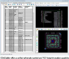
With advanced PDF extraction of vendor component data sheets, EDABuilder automates creation of schematic symbols and corresponding PCB footprints/land patterns. Data can be extracted from complex tables and diagrams, and pin assignments can be made to pin interface groups in automatic and interactive modes. Other functions include ability to select and drop between pin tables and symbol, assign and partition pins to symbols, and move pins onto symbols, between symbols, and back to spreadsheet.
Original Press Release:
EMA Automates the Library Creation Process for Engineers and PCB Designers
Rochester, NY - EMA Design Automation(TM) (www.ema-eda.com), one of the world's largest Electronic Design Automation Value Added Resellers, announced the release of EDABuilder, an application automating the creation of both schematic symbols and the corresponding PCB footprints / land patterns, reducing library creation to a fraction of the time.
"Creating schematic symbols and PCB footprints is a constant challenge," said Manny Marcano, president and CEO of EMA. "The traditional process is laborious, time consuming, and error prone. We created EDABuilder so that our customers could spend more time focusing on actual conceptual design rather than on mundane administrative tasks. Helping recover 'engineering time' is the best return on investment that we can provide."
EDABuilder contains the most advanced PDF extraction of vendor component data sheets. Data can be extracted from complex tables and diagrams, including BGA maps or SOIC diagrams. Content and data structures are extracted in minutes, versus days with a manual approach. Intelligent symbol partitioning allows a designer to use a higher level of abstraction to assign the symbol pins. Pin assignments can be made to pin interface groups in both automatic and interactive modes. Other functions include an easy to use select and drop between pin tables and the symbol, assign and partition the pins to symbols, as well as the ability to move pins onto the symbols, between symbols, and back to the spreadsheet.
PCB footprint generation fully supports both the IPC-7351 standard and user defined requirements across a broad range of component families. The process, driven by rules, settings, and form entered component dimensioning, accurately builds parts in a consistent and repetitive process. Footprint pads can be chosen from D-shape, oblong, or rectangular. Additionally, users can customize a specific pad shape with rounding or chamfering specifications. Pad stacks are user configurable and can be assigned to unique locations including corner pads or specific row/column positions.
Providing a single environment for PCB library generation avoids the common problem of mismatched symbol and footprint models. All too often, discrepancies between symbols and footprints are found in the middle of the design process leading to lost time and costly rework. This is a hard problem to solve since most design teams build their schematic and PCB libraries using separate tools making verification difficult. EDABuilder ensures that the symbol and footprint match from the start with its unified design environment, easy cross probing, and rigorous verification checks. This level of integration between the PDF data sheet, schematic symbol, and PCB footprint represents the next advancement in the library development process.
"With built-in exports to the Cadence OrCAD and Allegro Design Flows, along with optional exports for a host of other tools, design teams can take advantage of the cost and time savings inherent in a single source, multiple export library creation flow," added Marcano.
EMA is hosting a webinar to demonstrate EDABuilder and its unique capabilities. EDABuilder is available now starting at $2,495. To sign up for the webinar or for more information, visit us at www.ema-eda.com/EDABuilder or call 800-813-7494.
About EMA Design Automation, Inc.
EMA Design Automation is a value added innovator offering a complete range of electrical and mechanical CAD tools, product lifecycle management systems, services, training, and technical support. EMA is a Cadence® Channel Partner serving all of North America, an Autodesk Authorized Value Added Reseller, and is an Authorized North American Distributor of Aldec® Active-HDL(TM). EMA manufactures the Component Information Portal(TM) (CIP), TimingDesigner®, and CircuitSpace, and all are distributed through a worldwide network of value added resellers. EMA is a privately held corporation headquartered in Rochester, New York. Visit EMA at www.ema-eda.com for more information.
EMA Design Automation and Component Information Portal are trademarks, and TimingDesigner and CircuitSpace are registered trademarks of EMA Design Automation, Inc.
Cadence and OrCAD are registered trademarks of Cadence Design Systems, Inc.
Aldec and Active-HDL are registered trademarks of Aldec, Inc.
All other trademarks in this release are the property of their respective owners.