Double Side Lapping System aids silicon wafer manufacturing.
Share:
Press Release Summary:
Equipped with 2,100 mm OD lapping wheel, AC-2100L microLine® can process up to twenty 300 mm prime silicon wafers in one batch with sub-micron precision. It can also process up to eight 450 mm wafers. Along with independently driven inner and outer pin rings, features include automatic force calibration, in-situ wafer thickness metrology, and contactless gauges. Latter controls lapping wheel gap dimension, ensuring repeatable within-batch and batch-to-batch wafer thickness.
Original Press Release:
Novellus' Peter Wolters Subsidiary Introduces the AC-2100L microLine® Double Side Lapping System for Silicon Wafer Manufacturing
Innovative Technology Processes Twenty 300 mm Wafers in a Single Batch with Sub-micron Flatness
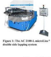
SAN JOSE, Calif. -- Novellus Systems (Nasdaq: NVLS) announced today that its subsidiary Peter Wolters GmbH has introduced a new version of its microLine double side lapping system for prime silicon wafers. The new AC-2100L system (Figure 1) features independently driven inner and outer pin rings, automatic force calibration, and in-situ wafer thickness metrology for closed-loop process control. The system can process up to twenty 300 mm wafers in one batch, while exceeding the latest wafer geometry requirements.
Double side lapping is becoming the technology of choice for prime silicon wafer manufacturing due to its combination of high throughput, precise wafer geometry control, and lower cost of consumables. Peter Wolters engineers have incorporated several innovative features into the new AC-2100L lapping system. Independently-driven inner and outer pin rings (Figure 2) enable maximum process control. Automatic force calibration compensates for weight loss of the upper lapping wheel due to typical process wear, ensuring accurate force control over the entire wheel life. Contactless gauges control the lapping wheel gap dimension, thus ensuring repeatable within-batch and batch-to-batch wafer thickness throughout the lapping process. Additionally, the system can be configured with a non-contact, optical gauge developed by Peter Wolters for in-situ measurement and control of wafer thickness. This industry-first technology provides wafer manufacturers with the sub-micron precision (Figure 3) required to meet leading-edge wafer geometry requirements.
The AC-2100L's high productivity is enabled by its new, larger lapping wheel, which has an outside diameter of 2100 mm. The larger wheel allows the use of five carrier rings, resulting in a twenty wafer batch size. For ease of cleaning, maintenance and wheel replacement, the machine head on the AC-2100L swivels out to provide service access to the lapping components. Existing Peter Wolters customers will recognize the user-friendly operator interface (HMI), which is based on the well-established AC-2000 platform.
"The new AC-2100L system will provide our prime wafer manufacturers with the ideal combination of high productivity, process flexibility, and precise control of the lapping process," said Kay Petersen, chief executive officer of Novellus' Industrial Applications Group. "While designed for today's 300 mm wafers, the AC-2100L can also simultaneously process up to eight 450 mm wafers, thus preparing Peter Wolters' customers for the next wafer size transition."
For more information about the AC-2100L, please visit novellustechnews.com
About Peter Wolters:
Peter Wolters GmbH, part of Novellus' Industrial Applications Group, is the leading manufacturer of high precision surface polishing systems for substrates made of silicon, sapphire, gallium arsenide, silicon carbide and other materials used to manufacture microelectronic, micro-optical, and micromechanical devices. Peter Wolters is headquartered in Rendsburg, Germany. For more information on Peter Wolters, please visit www.peter-wolters.com
About Novellus:
Novellus Systems, Inc. (Nasdaq: NVLS) is a leading provider of advanced process equipment for the global semiconductor industry. The company's products deliver value to customers by providing innovative technology backed by trusted productivity. An S&P 500 company, Novellus is headquartered in San Jose, Calif. with subsidiary offices across the globe. For more information, please visitwww.novellus.com
microLine is a registered trademark of Peter Wolters GmbH, and Novellus is a registered trademark of Novellus Systems, Inc.