DKN Research Provides Fine Silver Trace Technology Down to 50 Micron
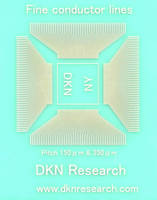
DKN Research, a leading engineering firm specializing in micro electronics and packaging technology is can now provide a fine thick film circuit technology down to 50 micron line/space. This is possible through an advanced screen-printing process using special silver inks and related materials that include substrates and insulating materials as the fundamental technology for Printable Electronics.
Polymer thick film circuits were always considered an economical solution, but performance levels from the printed circuit technology were sub par due to poor resolution and electrical conductivity. Traditional thick film circuits were intended for typical low end items such as keyboard membrane switches and touch panels on microwaves. Technical advances with ink materials and printing equipment over the last few years has trickled down, and the wiring capabilities from the new thick film circuits are closer to traditional etched copper circuits.
DKN Research developed an "Advanced Screen-Printing Technology" and can build functional thick film circuits by partnering with equipment and material manufacturers. DKN's Advanced Screen-Printing Technology can produce fine silver traces down to 30 micron lines and spaces for double and multilayer circuits with 80 micron via holes. The conductivity of the new silver traces is one order higher compared to traditional thick film circuits. Surprisingly, the conductor traces are available for soldering, unlike traditional polymer thick film circuits where soldering is impossible. Additionally, the new Advanced Screen-Printing Technology makes it possible to build embedded passive components and EL based optical components on flexible substrates. The Advanced Screen-Printing Technology is valuable in building new electronic devices such as high-density touch panel switches, functional sensor modules, large size signboards, flexible displays and more. The technology is also beneficial to build additional fine conductive traces on other circuit devices including multi-layer rigid boards, flexible circuits, ceramic circuits and monolithic IC chips.
Phase 1 of DKN Research's introduction for Advanced Screen-Printing Technology will provide a series of engineering services for fine line generation process down to 50 micron line/space with low resistance built on flexible substrates. A suitable combination of materials is needed that includes both insulation and substrate materials. DKN Research inventories a broad range of materials, and can supply appropriate materials according to the application. DKN Research can conduct prototype and mid volume fine line thick film circuit production as a part of the engineering service with its cooperating partner companies.
DKN Research welcomes all inquiries relative to learning the process and executing technical applications using their Advanced Screen-Printing Technology to create your own circuit devices. Please click on our link for more information www.dknresearch.com, or contact us at sales@dknresearch.com for detailed technical information and circuit samples.
DKN Research LLC,
62 Adams St.,
Haverhill, Massachusetts 01830-6862 U.S.A.
Phone: 1-978-436-1417 (Customer Service)
URL: www.dknresearch.com