Defect Inspection System handles wafers up to 300 mm.
Press Release Summary:
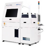
Designed for semiconductor, MEMS, and LED facilities, NSX® 220 Automated Macro Defect Inspection System uses gray-scale image analysis with color image capture for inspection and metrology in final manufacturing applications. It can detect scratches, mechanical damage, foreign materials, voids, and probe damage, while also performing 2D measurements on bumps, probe marks, and edge trim processes. System operates over 10–0.5 µm resolutions with brightfield and optional darkfield illumination.
Original Press Release:
Rudolph Adds NSX 220 System to Macro Defect Inspection Family
The new NSX tool is designed for semiconductor, MEMS and LED packaging and test facilities to achieve productivity at a low price point
Flanders, New Jersey —Rudolph Technologies, Inc. (NASDAQ: RTEC) today announced the availability of its new NSX® 220 Automated Macro Defect Inspection System. The system provides fast, easy defect inspection for traditional back-end processes in the semiconductor, MEMS and LED market at a reduced price point. The NSX 220 System joins the established NSX 320 System in the NSX family of automated macro defect inspection and metrology systems for final manufacturing facilities. The first NSX 220 System was installed in July at a major outsourced assembly and test (OSAT) facility in Asia.
“The NSX 220 System is a streamlined version of our NSX 320 System,” said Mike Jost, vice president and general manager of Rudolph’s Inspection Business Unit. “The NSX 220 System is designed for traditional macro defect inspection of wafers up to 300mm at conventional semiconductor, MEMS and LED final manufacturing facilities, while the NSX 320 System serves next-generation advanced packaging processes with defect inspection and three-dimensional metrology for wafers up to 450mm. The NSX 220 System benefits from many of the hardware and software innovations that made the NSX 320 System the market leader in advanced packaging, but is targeted for back-end facilities that do not need the full suite of capabilities offered by the NSX 320 System. Adding the NSX 220 System to the NSX family gives our customers a choice of best-in-class capabilities.”
The NSX 220 is an automated macro defect inspection system that uses gray-scale image analysis (with color image capture) to provide fast, accurate inspection and metrology in final manufacturing applications for wafers up to 300mm in size. It can detect traditional advanced macro defects such as scratches, mechanical damage, foreign materials, voids and probe damage, while also performing two-dimensional measurements on bumps, probe marks and edge trim processes. The system operates over a range of resolutions (10µm - 0.5µm) with both brightfield and optional darkfield illumination. The software platform, leveraged from the NSX 320 System’s success, uses host-based image processing and delivers significant improvements in usability and productivity over older-generation NSX Series equipment. Using centrally-managed recipe creation and editing, multiple NSX 220 tools can share a single recipe and be matched across the fab.
An optional suite of yield management software optimizes the productivity of both the NSX 220 and 320 Systems and minimizes the need for operator assistance. Discover® Software is designed for use with Rudolph inspection systems to allow real-time analysis for faster solutions and intelligent defect sampling for reduced offline review.
For more information about the NSX 220 Inspection System, visit www.rudolphtech.com or the Rudolph booth at SEMICON® Taiwan, September 4-6, 2013.
About Rudolph Technologies
Rudolph Technologies, Inc. is a worldwide leader in the design, development, manufacture and support of defect inspection, advanced packaging lithography, process control metrology, and data analysis systems and software used by semiconductor device manufacturers worldwide. Rudolph provides a full-fab solution through its families of proprietary products that provide critical yield-enhancing information, enabling microelectronic device manufacturers to drive down the costs and time to market of their products. The Company’s expanding portfolio of equipment and software solutions is used in both the wafer processing and final manufacturing of ICs, and in adjacent markets such as FPD, LED and Solar. Headquartered in Flanders, New Jersey, Rudolph supports its customers with a worldwide sales and service organization. Additional information can be found on the Company’s website at www.rudolphtech.com.
Trade Press:
Amy Pauling
952.259.1794
amy.pauling@rudolphtech.com