Clock IC optimizes JESD204B serial interface functionality.
Share:
Press Release Summary:
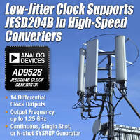
Intended for GSPS data converter applications, Model AD9528 delivers low-power, multi-output, clock distribution function with low-jitter performance, along with on-chip, 2-stage PLL and VCO. Device provides JESD204B-compatible subclass 1 SYSREF and deterministic latency clocking signals and supports options for SYSREF signal generation. When connected to recovered system reference clock and VCXO, AD9528 generates 12 low-noise outputs from 1–400 MHz, and 2 high-speed outputs at up to 1.25 GHz.
Original Press Release:
Low-Jitter 1.25-GSPS Clock Optimizes JESD204B Serial Interface Functionality in GSPS Data Converter Applications
New clock IC enables the unique functionality of the JESD204B SERDES high-speed interface
NORWOOD, Mass. -- Analog Devices, Inc. (NASDAQ: ADI) introduced today the AD9528 JESD204B clock and SYSREF generator defined to support the clock requirements for long-term evolution (LTE) and multicarrier GSM base station designs, defense electronics systems, RF test instrumentation, and other emerging wideband RF GSPS data acquisition signal chains. The use of the JESD204B standard for the high-speed converter-to-digital processor interface is becoming increasingly prevalent across many state-of-the-art applications as data rates are being pushed into the multi-Gb/s range, and multi-channel synchronization and data latency management are becoming a system necessity. The JESD204B interface was specifically developed to address high-data rate system design needs, and the AD9528 clock device contains functions that support and enhance the unique capabilities of that interface standard.
The AD9528 provides a low-power, multi-output, clock distribution function with low-jitter performance, along with an on-chip, two-stage PLL and VCO. The on-chip VCO tunes from 3.6 GHz to 4.0 GHz, with the input receivers and oscillator providing both single-ended and differential operation.
Download AD9528 data sheet, order samples and evaluation boards: http://www.analog.com/AD9528
Connect with engineers and ADI product experts on EngineerZone™, an online technical support community: http://ez.analog.com/
Find application notes and technical articles about wireless and communications solutions from ADI: http://communications.analog.com/en/segment/cmmn.html
Explore ADI’s Wideband RF Signal Processing website: http://www.analog.com/widebandRF
Visit ADI’s JESD204B interface design resource page: http://www.analog.com/JESD204B
The AD9528 provides JESD204B-compatible subclass 1 SYSREF and deterministic latency clocking signals and supports a variety of options for SYSREF signal generation. The most basic is a simple buffer function wherein the user-provided SYSREF signal is fanned out to the SYSREF output pins. When provided with an external SYSREF source, the AD9528 is also capable of synchronizing the SYSREF outputs to the clock outputs being generated internally, which is necessary to achieve accurate deterministic latency. The AD9528 is also capable of generating the SYSREF source internally. The AD9528 supports both continuous signal SYSREF generation and “n-shot” pulse generation. N-shot generation is vital in systems where a continuous signal might result in unwanted spurs in the output spectrum of the data converter being clocked.
When connected to a recovered system reference clock and a VCXO, the AD9528 generates 12 low-noise outputs with a range of 1 MHz to 400 MHz, and two high-speed outputs at up to 1.25 GHz. The frequency and phase of one clock output relative to another clock output can be varied by means of a divider phase-select function that serves as a jitter-free, coarse timing adjustment in increments that are equal to half the period of the signal coming from the VCO output. The SYSREF signals each have additional phase offset capability making it easy to dial-in the optimal arrival time at each target device.
Pricing and Availability
Product | Sample Availability | Full Production | Price Each Per 1K | Packaging |
AD9528BCPZ | NOW | NOW | $8.25 | 72-lead LFCSP |
AD9528/PCBZ Evaluation Board | NOW | NOW | Â $190.00 | n/a |
                          Â
The AD9528 can be designed into wideband RF data acquisition applications with ADI’s AD9680 dual-channel, 14-bit, 1.0-GSPS JESD204B A/D converter.
About Analog Devices
Innovation, performance, and excellence are the cultural pillars on which Analog Devices has built one of the longest standing, highest growth companies within the technology sector. Acknowledged industry-wide as the world leader in data conversion and signal conditioning technology, Analog Devices serves over 100,000 customers, representing virtually all types of electronic equipment. Analog Devices is headquartered in Norwood, Massachusetts, with design and manufacturing facilities throughout the world. Analog Devices is included in the S&P 500 Index.
EngineerZone is a trademarked term of Analog Devices, Inc.
Subscribe to ADI's News Feed
Follow ADI on Twitter
To subscribe to Analog Dialogue, ADI's monthly technical journal, visit: http://www.analog.com/subscribe.