Chemical Resistant Plastics target CMP applications.
Share:
Press Release Summary:
Intended for semiconductor industry, TECATRON® CMP and TECAPEEK® CMP have been specifically developed for components used in chemical mechanical planarization process, which involves use of different slurries. TECATRON PPS material demonstrates abrasion and wear resistance, while PEEK material additionally offers high ductility and dimensional stability. Since minimal degree of deburring work is required, productivity is optimized.
Original Press Release:
Ensinger Unveils Two High-Performance Plastics for CMP Applications
Plastics processor Ensinger will be launching two new materials for the semiconductor industry in time for the Semicon Fair in Taiwan
The new TECATRON® CMP and TECAPEEK® CMP product lines have been developed specifically for components used in the chemical mechanical planarization process (CMP). One of the key steps used in silicon wafer production, CMP imposes stringent demands on the mechanical properties and chemical resistance of high-performance plastics.
The CMP process involves the use of different slurries which take a heavy toll on the handling components used. The new PPS material, TECATRON CMP, demonstrates higher abrasion and wear resistance compared to the predecessor product. In combination with material-specific resistance to chemicals and solvents, these improved tribological properties help extend the service life of the plastic components used, with reduced placement and downtimes resulting in lower costs per wafer.
The use of special slurries can bring about extreme mechanical loads. Under these tough conditions, TECAPEEK CMP provides the ideal material. This new PEEK product from Ensinger is characterized not only by its higher ductility and dimensional stability, but also by its excellent resistance to wear and abrasion. In association with a high level of chemical resistance, these outstanding mechanical and tribological properties make for a significantly extended service life.
The benefits of the new material are brought to bear as early as the semi-finished material processing stage, with improved machinability making for shorter processing times. Productivity is also significantly improved by the minimal degree of deburring work required.
Applications in wafer production
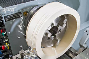
Ensinger’s two new latest developments are ideally suited for the manufacture of retaining rings. These components require extreme processing precision and dimensional stability in order to reduce the occurrence of microscratches in wafers and ensure a higher yield of usable ICs. Extensive tests carried out by machining companies and leading OEMs have confirmed the material benefits of the new thermoplastic materials.
Ensinger produces semi-finished products for CMP applications in its parent plant in Nufringen, Germany. It supplies extruded tubes from stock in dimensions and tolerances adapted to meet the special demands of the semiconductor industry.
Quality management
Ensinger is certified to ISO 9001:2008 and has implemented a quality management system compliant with international standards. Because the manufacture of products for the semiconductor industry calls for particularly meticulous care, the documentation and traceability procedures in place at Ensinger include all raw materials and manufacturing steps.
For more information contact Larry Resavage 1-800-243-3221.
The Ensinger group is engaged in the development, manufacture and sale of compounds, semi-finished materials, profiles and technical parts made of engineering and high performance plastics through extrusion, machining and injection moulding. With a total of 2,100 employees at 27 locations, the family-owned enterprise is represented worldwide in all major industrial regions with manufacturing facilities or sales offices.