Characterization System aids materials science research.
Press Release Summary:
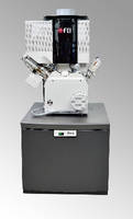
Capable of seeing structure and composition and adding/removing material at nanometer scale, Helios NanoLab™ G3 DualBeam™ allows scientists to explore fundamental relationships between structure and function. CX configuration offers versatile sample handling and positioning for flexible analysis, sample preparation, and characterization, while UC configuration delivers increased sensitivity to surface detail and optimized performance on soft, non-conductive, or beam-sensitive materials.
Original Press Release:
FEI Releases New Helios NanoLab G3 DualBeam
Next generation DualBeam extends Helios performance leadership while enhancing usability with a new user interface and workflow-specific configurations.
Hillsboro, Ore. — FEI (NASDAQ: FEIC) announced today the release of the next generation of its industry-leading Helios NanoLab™ DualBeam™. The Helios NanoLab G3 DualBeam extends the Helios family’s leadership position with unmatched image contrast and resolution, while at the same time, adding a new, easy-to-use user interface. The new Helios comes in two different workflow-specific configurations for materials science research. It will be featured in the FEI booth at the International Microscopy Congress, September 7-12, in Prague, Czech Republic.
“The Helios NanoLab G3 DualBeam continues FEI’s well-established leadership in DualBeam instrumentation, building on a long history of performance and innovation from the first commercial DualBeam, which FEI launched more than 20 years ago, to the Helios PFIB™ DualBeam just announced at the Microscopy and Microanalysis show last month,” said Trisha Rice, vice president and general manager of Materials Science for FEI. “This third generation of the Helios family continues to provide the high resolution and strong image contrast that the family is known for, but adds a new interface that can actually guide the user through typical operations. We have optimized each of the configurations for a particular class of workflows, based on customer feedback and our long and deep involvement in DualBeam analysis.”
The DualBeam instruments’ ability to see structure and composition and add and remove material at the nanometer scale allows materials scientists to explore fundamental relationships between structure and function and prepare ultrathin samples for atomic scale analysis in transmission electron microscopes (TEM).
The CX configuration of the Helios NanoLab G3 DualBeam includes more versatile sample handling and positioning for fast, flexible analysis, sample preparation and characterization. The UC configuration delivers the ultimate imaging capability with increased sensitivity to surface detail and improved performance on soft, non-conductive or beam-sensitive materials.Â
Please visit www.fei.com/helios-g3 for more information, or stop by the FEI booth (#6) at the International Microscopy Congress.
About FEI
FEI Company (Nasdaq: FEIC) designs, manufactures and supports a broad range of high-performance microscopy workflow solutions that provide images and answers at the micro-, nano- and picometer scales. Its innovation and leadership enable customers in industry and science to increase productivity and make breakthrough discoveries. Headquartered in Hillsboro, Ore., USA, FEI has over 2,600 employees and sales and service operations in more than 50 countries around the world. More information can be found at: www.fei.com.