Bruker Wins Over $7 Million in SP9900+ 3D Optical Microscope Orders
Share:
Instrument Breaks the Throughput Barrier for HDI Substrate Metrology
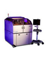
TUCSON, AZ - Bruker announced today that it has already received more than $7 million in orders for its new Bruker SP9900+ high-throughput high density interconnect (HDI) substrate metrology system, and has begun shipping the product in volume. The SP9900+ Large Format 3D Optical Microscope is specially designed for the semiconductor packaging industry and offers major advantages over previous generations of optical microscope technology. Dramatic improvements in inspection throughput are provided by the system's aerial coverage of up to 600x600 millimeters and traverse speeds up to 50 millimeters per second.
"Manufacturers of multichip modules (MCM) and high pin count semiconductor chips are continually increasing panel sizes, reducing feature sizes and increasing the pin count of their products, which creates new challenges in process control for high-volume production," said Mark R. Munch, President, Bruker MAT Group and Bruker Nano Surfaces Division. "The most important areas typically involve measurement of traces, vias, and interconnects, as well as the surface roughness of copper and Ajinomoto build-up film. Working closely with our customers, we've been able to reduce the 'time to measurement' for these critical inspection challenges to less than one half of previous generation systems."
"The new SP9900+ provides radical improvements in measurement speed due to its faster traverse speeds, faster autofocusing, faster camera, revolutionary fixture-loading mechanism and augmented auto intensity function," added Rob Loiterman, Executive Vice President and General Manager of Bruker's Stylus and Optical Metrology Business. "We've optimized the system to maximize factory throughput while ensuring the most accurate measurements which should help our customers improve yield and keep lowering the cost of consumer electronics."
About SP9900+ HDI Substrate Metrology System
The SP9900+ incorporates years of packaging and panel measurement experience to provide unprecedented speed, metrology capability, reliability, serviceability, and manufacturing readiness for 3D critical dimension measurements in MCM and HDI printed circuit board (PCB) applications. Bruker 3D Optical microscopes feature Vision® operating and analysis software, and the industry's most intuitive, modular user interface to deliver user-level-customization capabilities for the widest possible range of surface profiling metrology applications. The SP9900+ utilizes a revolutionary gantry design to deliver results in a 600x600-millimeter measurement envelope. Moreover, the SP9900+ delivers all these benefits within virtually the same footprint as previous generation SP profilers.
About Bruker Corporation (NASDAQ: BRKR)
Bruker Corporation is a leading provider of high-performance scientific instruments and solutions for molecular and materials research, as well as for industrial and applied analysis. For more information about Bruker Corporation, please visit www.bruker.com.