Automated Macro Defect Inspection System suits TSV processes.
Press Release Summary:
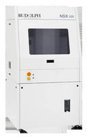
Designed for packaging processes that use through silicon vias (TSV) to connect multiple die in one package, NSX® 320 provides inspection capabilities for edge trimming metrology, wafer alignment during bonding processes, sawn wafers on film frames, and other processes. Incorporated XSoft(TM) system software capabilities include high-speed staging and on-the-fly image capture as well as range of sensor and objective options. Additionally, system can flip wafers for front/back inspection.
Original Press Release:
Rudolph Receives First Order for NSX 320 Automated Macro Defect Inspection System for TSV Processes
Latest addition to industry-leading NSX family delivers superior performance in
advanced back-end processes used to connect multiple die in a single package.
Flanders, New Jersey-Rudolph Technologies, Inc. (NASDAQ: RTEC), a leading provider of process characterization equipment and software for wafer fabs and advanced packaging facilities, announced today the availability of the new NSX® 320 Automated Macro Inspection System designed specifically for advanced packaging processes that use through silicon vias (TSV) to connect multiple die in a single package. The system also provides critical inspection capabilities for edge trimming metrology, wafer alignment during bonding processes, sawn wafers on film frames and other TSV related processes. The company has received its first NSX 320 system order from one of the leading IC manufacturers.
"TSV technologies are really taking off as IC manufacturers seek to pack ever-increasing performance and functionality into smaller and smaller spaces," said Rajiv Roy, Rudolph's vice president of business development and director of back-end marketing. "The NSX 320 System addresses a common set of requirements defined by our customers in foundries, IDMs, fabless and equipment manufacturers. It provides critically- needed defect inspection capability for these radically new packaging processes-at full production throughputs and minimal cost of ownership."
In addition to industry-leading speed and sensitivity, the NSX 320 System incorporates Rudolph's proprietary XSoft(TM) system software capabilities-including high- speed staging, on-the-fly image capture and a wide range of sensor and objective options-for unprecedented flexibility and ease of use. New features engineered into the NSX 320 deliver more benefit to users than ever before, including the ability to perform critical dimension measurement; the addition of 3D sensors for TSV depth or bump metrology; and the ability to flip wafers to allow inspection of both front and back surfaces.
Rudolph's NSX Series inspection tools deliver production-proven, high-throughput macro defect inspection for back-end integrated circuit manufacturing processes. Macro defects (defects 0.5 micron and larger) can be created during wafer manufacturing, probing, bumping, dicing, or by general handling, and can have a major impact on the quality of a microelectronic device and the yield of the manufacturing process. The NSX quickly and accurately detects yield-inhibiting defects, providing quality assurance and valuable process information.
NSX System users have demonstrated the benefit of applying Rudolph's total solution-an integrated suite of yield management software designed for use with every Rudolph inspection system-to analyze, classify and review data to determine trends that ultimately affect yield.
For more information, please visit www.rudolphtech.com or email info@rudolphtech.com.
Rudolph Technologies, Inc. is a worldwide leader in the design, development, manufacture and support of defect inspection, process control metrology, and data analysis systems and software used by semiconductor device manufacturers worldwide. Rudolph provides a full-fab solution through its families of proprietary products that provide critical yield-enhancing information, enabling microelectronic device manufacturers to drive down the costs and time to market of their products. The company's yield management solutions are used in both the wafer processing and final manufacturing of ICs, as well as in emerging markets such as LED and Solar. Headquartered in Flanders, New Jersey, Rudolph supports its customers with a worldwide sales and service organization. Additional information can be found on the company's web site at www.rudolphtech.com.
Contacts:
Investors:
Steven R. Roth
973.448.4302
steven.roth@rudolphtech.com
Trade Press:
Virginia Becker
952.259.1647
virginia.becker@rudolphtech.com