Active Spread Spectrum Clock Generator ICs reduce EMI at source.
Share:
Press Release Summary:
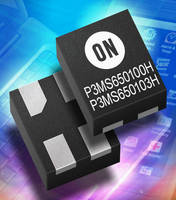
Supplied in 8-pin, 2 x 2 x 0.8 mm WDFN package, P3P8203A supports 3.3 V input, 18–36 MHz frequency range, and analog control of spread spectrum deviation via external resistor. Choice of external resistor value lets designers customize applications to achieve desired EMI reduction. Supplied in 4-pin, 1 x 1.2 x 0.8 mm WDFN package, P3MS650100H and P3MS650103H support 1.8–3.3 V input, 0.45%–1.4% typ spread spectrum deviations, and 15–60 MHz frequency range.
Original Press Release:
ON Semiconductor Introduces Active Spread Spectrum Clock Generator ICs for EMI Reduction in Portable, Consumer and Computing Applications
Spread spectrum clock generators conserve board space and support EMI regulatory compliance without expensive and time consuming redesigns
PHOENIX, Ariz. – ON Semiconductor (Nasdaq: ONNN), a premier supplier of high performance silicon solutions for energy efficient electronics, has introduced a new series of active spread spectrum clock generator integrated circuits (ICs) that manage electromagnetic interference (EMI) and Radio Frequency Interference (RFI) at the clock source, delivering system-wide EMI reduction of all clock dependent signals.
The P3P8203A LVCMOS peak EMI reduction clock generator targets applications such as graphics cards, computing and consumer applications. This device supports an input voltage of 3.3 V, a frequency range of 18 MHz to 36 MHz, and analog control of spread spectrum deviation by means of an external resistor. By choosing a different value of the external resistor to provide the desired amount of spread spectrum deviation at the output, system designers now have the added flexibility to customize their applications to achieve the desired EMI reduction. The P3P8203A is housed in an 8-pin, 2 mm x 2mm x 0.8 mm WDFN package, making it ideal for use in PCB space constrained applications. Operating temperature range is 0°C to +70°C.
The P3MS650100H and P3MS650103H LVCMOS peak EMI reduction clock generators are ideal for use in PCB space constrained applications such as portable, battery powered devices – including mobile phones and tablets where EMI/RFI can be a significant challenge and compliance with regulations is a prerequisite. Housed in a miniature four-pin WDFN package measuring 1 mm x 1.2 mm x 0.8 mm, these versatile new devices are spread spectrum clock generators that provide the industry’s smallest standalone active solution for reducing EMI/RFI at the clock source as well as downstream clock and data signals derived from the clock source. The P3MS650100H and P3MS650103H support input voltages ranging from 1.8 volts (V) to 3.3 V, typical spread spectrum deviations of 0.45 percent to 1.4 percent, and reduction of EMI/RFI in clock sources with a frequency range of 15 megahertz (MHz) to 60 MHz. Operating temperature range is -20ºC to +85ºC.
“The need to achieve EMI regulatory compliance while controlling costs and minimizing PCB real estate is a significant challenge for mobile and computing applications,” said Ryan Cameron, vice president of Industrial and Timing Products at ON Semiconductor. “Our new EMI reduction ICs address these challenges on all fronts by providing a cost-effective solution that reduces EMI/RFI at the source and at all downstream clock and data signals derived from the source. By implementing these devices early in the design cycle, design engineers potentially avoid the need for alternate solutions and the inclusion of costly additional PCB layers or shielding to deal with EMI/RFI problems.”
Packaging and Pricing
The P3P8203A is offered in an eight-pin WDFN package and is priced at $0.44 per unit in 10,000 unit quantities. The P3MS650100H and P3MS650103H are offered in a four-pin WDFN package and are priced at $0.24 per unit in 10,000 unit quantities.
Electronica 2012
Visit ON Semiconductor at Electronica 2012, Nov. 13-16, Hall A5, Stand 225 for a demonstration of the P3P8203A and other power, thermal and signal management solutions for communications applications.
About ON Semiconductor
ON Semiconductor (Nasdaq: ONNN) is a premier supplier of high performance silicon solutions for energy efficient electronics. The company's broad portfolio of power and signal management, logic, discrete and custom devices helps customers efficiently solve their design challenges in automotive, communications, computing, consumer, industrial, LED lighting, medical, military/aerospace and power applications. ON Semiconductor operates a world-class, value-added supply chain and a network of manufacturing facilities, sales offices and design centers in key markets throughout North America, Europe, and the Asia Pacific regions. For more information, visit www.onsemi.com.
ON Semiconductor and the ON Semiconductor logo are registered trademarks of Semiconductor Components Industries, LLC. All other brand and product names appearing in this document are registered trademarks or trademarks of their respective holders. Although the company references its Web site in this news release, such information on the Web site is not to be incorporated herein.
Contacts
Beth Johnston
Marketing Communications Specialist
ON Semiconductor
(208) 234-6738
beth.johnston@onsemi.com
Ken Rizvi
MA, Treasury & Investor Relations
ON Semiconductor
(602) 244-3437
ken.rizvi@onsemi.com
Issued by:
Simon Krelle, Pinnacle Marketing Communications Ltd
Tel: (339) 368 6122Â Â Â Â Â Â Â Â Â Â Â Â Â Â Â Â Â Â Â Â Â Â Â Â Â Â Â
Email: s.krelle@pinnaclemarcom.com
Web: www.pinnacle-marketing.com