Saki Demonstrates 3D SPI, AOI, AXI, and 2D Bottom-Side AOI at IPC APEX Expo Booth 1407
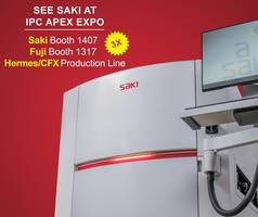
Fremont, CA - 22 January 2019 - Saki Corporation, an innovator in the field of automated optical and x-ray inspection and measurement equipment, will present its 3D solder paste inspection (SPI), automated optical inspection (AOI), and automated x-ray inspection (AXI) systems, plus new 2D Bottom-side AOI, at IPC APEX Expo 2019, January 29-31, at the San Diego Convention Center, San Diego, CA, at booth #1407. In addition, Saki's M2M communication/Industry 4.0/Smart Factory capabilities will be on display in the Fuji booth #1317 and in the Hermes/CFX production line.
Saki's 3Di Series is the fastest AOI system in the industry. It has scalable resolutions of 7µm, 12µm, and 18µm, closed-loop functionality, and a sturdy frame with a dual-drive system, resulting in accuracy, stability, and reliability.
Demonstrations of Saki's new version of Saki Self-Programming Software (SSP), the inspection industry's first self-programming software, will be given. With Saki Self-Programming Software, no programming is necessary, no golden board is needed, and programming errors are eliminated.
New at IPC APEX is Saki's 2D Bottom-side AOI System. Saki's proprietary 2D high-speed imaging technology scans an entire 460 x 510mm printed circuit board assembly in one pass, capturing its image on-the-fly, in real time, storing the image into memory, and creating inspection data for the entire board. Saki's bottom-side AOI system ensures PCB quality after dip, selective, and wave soldering. The system completely automates bottom-side inspection, including pin through-hole fillets. It's fast, cost-effective, and eliminates the need for flipping the PCB.
Saki's new 3D SPI and AOI systems have 12 megapixel cameras for the fastest inspection and highest resolution with high accuracy and repeatability. They offer closed-loop functionality and 2D and 3D inspection using an LCoS imaging system. Both systems are hardware compatible and come with Saki Self-Programming Software.
Previews will also be given of Saki's new 3D AXI system. The system benefits from the technology advancements of Planar Computer Tomography that perfectly separates top and bottom sides of the PCB and takes continuous 3D images without joints. With a programmable resolution from 13-30µm and best-in-class Cpk and gage repeatability and reproducibility, it delivers 100% head-in-pillow detection. Saki's AXI has been employed in the semiconductor industry for inspection and measurement of insulated gate bipolar transistors (IGBTs) and land grid arrays (LGAs).
"The past year has seen lots of changes, growth, and new equipment and technologies at Saki," said Satoshi Otake, general manager of Saki America. "We are excited to share our news and developments with the electronics community. Please make an appointment on our website (www.sakiglobal.com) or stop by our booth to find out more."
For more information or to make an appointment contact Saki at 1.510.556.6459, email sales.us@sakiglobal.com, or visit our website at www.sakiglobal.com.
About Saki Corporation
Since its inception in 1994, Saki has led the way in the development of automated recognition through robotic vision technology. Saki's 3D automated solder paste, optical, and x-ray inspection systems (SPI, AOI, AXI) have been recognized to provide the stable platform and advanced data capture mechanisms necessary for true M2M communication, improving production, process efficiency, and product quality. Saki Corporation has headquarters in Tokyo, Japan, with offices, sales, and support centers around the world.
For more information contact:
Satoshi Otake - General Manager
Saki America, Inc.
Phone: +1.510.556.6459
E-mail: ohtake.satoshi@sakicorp.com
Andrea Roberts
AR Marketing, Inc. (agency)
Phone: +1 858-204-9584
Email: andrea@armarketinginc.com