KLA-Tencor Introduces New Metrology Systems for Leading-Edge Integrated Circuit Device Technologies
Comprehensive Process Control Facilitates Advanced Multi-Patterning Techniques and EUV Lithography
MILPITAS, Calif., Feb. 22, 2017 - KLA-Tencor Corporation (NASDAQ: KLAC) today introduced four innovative metrology systems that enable development and high-volume manufacturing of sub-10nm integrated circuit (IC) devices: the Archer™ 600 overlay metrology system, the WaferSight™ PWG2 patterned wafer geometry measurement system, the SpectraShape™ 10K optical critical dimension (CD) metrology system and the SensArray® HighTemp 4mm in-situ temperature measurement system. These four new systems expand the capability of KLA-Tencor's unique 5D Patterning Control Solution™ to support advanced patterning techniques, such as self-aligned quadruple patterning (SAQP) and extreme ultraviolet (EUV) lithography.
"Leading-edge device manufacturers are facing extremely tight patterning specifications," said Oreste Donzella, chief marketing officer at KLA-Tencor. "To understand patterning errors, chipmakers need to quantify process variations, isolate their sources and fix the underlying issues. The new metrology systems announced today generate critical data that engineers can use to specify detailed scanner corrections in the lithography module and process improvements in etch, films and other modules. Our new overlay, patterned wafer geometry, optical critical dimension and in-situ temperature measurement systems serve key roles in driving 193i multi-patterning performance and baselining early EUV lithography results."
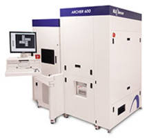
The Archer 600 extends imaging-based overlay metrology technology with new optics and novel measurement targets, helping chipmakers achieve sub-3nm overlay error for advanced logic and memory devices. Innovative ProAIM™ targets deliver better resilience to process variations and improved correlation between target and device overlay errors, producing more accurate overlay measurements. The Archer 600's new optical technologies, including a higher brightness light source and polarization module, enable tighter overlay error feedback and control across a range of process layers - from thin resists to opaque hard mask materials. With enhanced productivity, the Archer 600 supports increased sampling of overlay error for improved scanner corrections or identification of inline excursions. Multiple Archer 600 systems are already measuring the most advanced devices at foundry, logic and memory manufacturers worldwide.
The WaferSight PWG2 produces comprehensive wafer stress and shape uniformity data, enabling process tool monitoring and matching for film deposition, anneal, etch and other process modules. With significant productivity improvements, the WaferSight PWG2 promotes increased wafer sampling in production, helping chipmakers identify and fix process-induced wafer stress variations that can cause patterning and yield issues. The WaferSight PWG2's wafer shape data can also be fed forward to the lithography scanner to address overlay errors due to wafer stress, a particular concern for 3D NAND devices, which utilize thick film stacks that can distort wafers. With industry-unique vertical wafer hold, the WaferSight PWG2 measures front and back wafer surfaces simultaneously, generating wafer flatness and topography metrics that can improve prediction and control of scanner focus. Several WaferSight PWG2 systems are installed at advanced IC manufacturers, where they are used in development for lithography control, and in high volume manufacturing to optimize and monitor a wide range of fab processes.
The SpectraShape 10K optical-based metrology system measures the CDs and three-dimensional shapes of complex IC device structures following etch, chemical mechanical planarization (CMP) and other process steps. To comprehensively characterize device structures, the SpectraShape 10K employs a diverse array of optical technologies, including new polarization capability and multiple incidence angles for the ellipsometer, and a new high brightness light source with TruNI™ illumination for the reflectometer. These technologies enable accurate measurement of the numerous critical parameters associated with FinFET and 3D NAND devices - such as CD, height, SiGe shape and channel hole bow profile. With higher throughput than its predecessor, the SpectraShape 10K facilitates the increased sampling required for tighter process control and the growth in number of process layers due to multi-patterning techniques. The SpectraShape 10K has been strongly adopted by foundries for FinFET and multi-patterning integration, with additional systems supporting advanced 3D NAND fabrication at all the leading memory manufacturers.
Through in-situ measurements, the SensArray HighTemp 4mm wireless wafer provides temporal and spatial temperature information for advanced films processes. With a thinner wafer profile than its predecessor, the SensArray HighTemp 4mm is compatible with a wider range of process tool types, including track, strip and physical vapor deposition (PVD) systems. With a temperature range of 20 – 400°C, the SensArray HighTemp 4mm enables process characterization and tool qualification by mapping thermal variations that can affect process windows and patterning performance. Multiple SensArray HighTemp 4mm wafers are in use at microprocessor, DRAM and 3D NAND manufacturers for tuning and routine process monitoring of films applications.
The Archer 600, WaferSight PWG2, SpectraShape 10K and SensArray HighTemp 4mm are integrated with KLA-Tencor's 5D Analyzer® advanced data analysis system, which supports real-time process control and provides tools for engineering monitoring and analysis. To maintain the high performance and productivity demanded by IC manufacturing, the Archer 600, WaferSight PWG2, SpectraShape 10K and SensArray HighTemp 4mm are backed by KLA-Tencor's global comprehensive service network. More information on the four new systems can be found on the 5D Patterning Control Solution web page.
About KLA-Tencor:
KLA-Tencor Corporation, a leading provider of process control and yield management solutions, partners with customers around the world to develop state-of-the-art inspection and metrology technologies. These technologies serve the semiconductor, LED and other related nanoelectronics industries. With a portfolio of industry-standard products and a team of world-class engineers and scientists, the company has created superior solutions for its customers for more than 40 years. Headquartered in Milpitas, Calif., KLA-Tencor has dedicated customer operations and service centers around the world. Additional information may be found at www.kla-tencor.com (KLAC-P).
SOURCE KLA-Tencor Corporation
CONTACT: Investor Relations:
Ed Lockwood,
Sr. Director, Investor Relations,
(408) 875-9529,
Media Relations:
Becky Howland, Ph.D.,
Sr. Director, Corporate Communications,
(408) 875-9350,
Web Site: http://www.kla-tencor.com