FEI Connectivity Solutions Improve and Accelerate TEM Imaging for Semiconductor Manufacturing
Higher-quality results in hours (not days) speed process development and enhance yields
Hillsboro, Ore./July 15, - FEI Company (Nasdaq: FEIC), a leading provider of atomic-scale imaging and analysis systems, today announced the Ultimate Throughput(TM) and Ultimate Imaging(TM) Connectivity Solutions. By accelerating and improving the quality of preparation, imaging and analysis of the ultra-thin samples required for transmission electron microscopy (TEM), the FEI® Connectivity Solutions can reduce a lab's "wafers-to-atoms" time from days to hours. That, in turn, offers the opportunity to dramatically improve lab efficiency to better support the development of new processes and enhance yields.
"Nowhere is the saying 'time is money' more true than in the semiconductor manufacturing industry," said Tony Edwards, FEI's Electronics division general manager. "Multi-billion dollar fab investments result in tremendous pressure to take new products to market as fast as possible, and the cost of downtime in a high-volume production process can easily run to millions of dollars a day. The economic benefit provided by faster answers to critical process questions is substantial."
TEM usage has grown quickly in recent years, driven by the need for imaging and analysis of barrier layers, critical interfaces, gate structures, dopant profiles and silicon strain. TEM requires ultrathin samples that can take days to prepare using manual techniques. Sample preparation techniques using FEI focused ion beam (FIB) and SEM DualBeam(TM) systems are faster and more reliable. The FEI Connectivity Solutions improve the efficiency and quality of sample preparation by linking the operations of preparation, lift-out, transfer, loading and imaging/analysis tools.
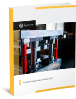
The Ultimate Imaging solution includes: the Helios NanoLab(TM) 400S DualBeam system for sample preparation and thinning, the MultiLoader(TM) tool for tweezer-less transfer and loading of mounted samples, and the Titan3(TM) TEM for sub-Angstrom imaging and analysis.
The Ultimate Throughput solution includes: the CLM-3D(TM) full wafer DualBeam system for reliable, repeatable, programmed TEM sample preparation; the TEMLink(TM) 150 ex-situ extraction tool for automated sample lift-out; and the MultiLoader(TM) tool and Cartridge Transfer Station for sample staging, transfer and loading to a TEM (for imaging and analysis) or to the Helios NanoLab 400S (for additional thinning). Both solutions use versions of the FEI AutoTEM(TM) software for precision in the location and preparation of the samples.
About FEI Company
FEI (Nasdaq: FEIC) is the world leader in pioneering technologies and applications that deliver imaging solutions for 3D characterization, analysis and modification/prototyping with resolutions down to the sub-Angstrom level. Our customers, working in advanced research and manufacturing, are supported by field-experienced applications specialists. They have open access to FEI's prestigious global user network so they can succeed in accelerating nanoscale discovery and contribute to better living through new product commercialization. FEI's NanoPorts in North America, Europe and Asia provide centers of technical excellence where our world-class community of customers and specialists collaborate on the ongoing development of new ideas and innovative solutions. FEI has sales and service operations in more than 50 countries around the world.
More information can be found at: www.fei.com.
For more information contact:
Media Contact:
Sandy Fewkes, Principal
MindWrite Communications, Inc
+1 408 224 4024
sandy@mind-write.com