Critical Link Announces Embedded Imaging Systems with Full Engineering Support
- Company will showcase its engineering support services and custom imaging design capabilities at SPIE’s Photonics West, Moscone Center, San Francisco, Jan. 30 - Feb. 1, 2018, in South Hall booth #210.
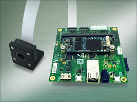
SYRACUSE, N. Y. - November 29, 2017 - Critical Link, LLC, experts in image sensor technology, system-on-chip (SoC) and field-programmable gate array (FPGA) designs, vision protocols, and signal processing, announces its full engineering support services to enhance the company’s product development and manufacturing capabilities. Specializing in embedded systems and custom imaging platforms, the company’s engineering team designs, manufactures, and supports sensor board development, on-board processing, and a wide variety of interfaces/ protocols for industrial applications including test and measurement, medical/scientific instrumentation, factory automation, transportation, and defense. Critical Link’s imaging platforms incorporate CMOS/sCMOS, CCD, indium gallium arsenide (InGaAs), and other sensor technologies, including 1D and 2D arrays.
Director of marketing, Amber Thousand, notes, “Our expert engineering team supports our customers at any step in their product development through manufacturing and the assembly process. We pride ourselves on our flexibility to provide the exact elements required, at the time needed, to meet our customer’s specifications. We offer a wide variety of engineering skills and services, but only deploy them as needed, which helps keep our customers’ costs under control.”
To learn more about Critical Link’s cost-effective, full engineering support services and product development, please go to: http://www.criticallink.com/services/ or stop by South Hall booth #210 at SPIE’s Photonics West, Moscone Center, San Francisco, Jan. 30 - Feb. 1, 2018. The company will be giving away two embedded imaging development kits and all booth visitors will be entered into the drawing for a chance to win a MitySOM-5CSX Vision Development Kit.
For more information about the company’s custom imaging design platforms, visit: http://www.criticallink.com/services/custom-imaging/. For details about Critical Link’s product development, including customizable system on modules (SOMs), development kits, board sets, image processing building blocks, interface options and more, please see: http://www.criticallink.com/products/.
ABOUT THE COMPANY:
Critical Link, LLC (Syracuse, NY www.criticallink.com), founded in 1997, develops embedded systems solutions, system on modules (SOMs) and imaging systems for a wide variety of electronic applications. As experts in image sensor technology, system on chip (SoC) and field-programmable gate array (FPGA) design, signal processing, and vision protocols, we support all product development tasks, from concept to final production.
Our flexibility allows us to deliver full lifecycle support and services at any step along the product development path, when and where needed, to effectively keep costs down. From engineering to hardware and software development, and mechanical engineering to prototyping and manufacture/assembly, Critical Link is committed to helping our OEM customers reach their project goals quickly and cost-effectively.
Privately held, Critical Link is a Platinum member of the Intel FPGA Design Services Network and Intel IoT Solutions Alliance, a Platinum Partner of the TI Design Network, and a certified member of the Arrow Consulting Engineering Services (ACES) network.