

Applied Materials, Inc.
Austin, TX 78724
Share:
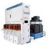
Dielectric Deposition System is designed for 3D chip packaging.
Applied ProducerÃ-® InVia(TM) dielectric deposition system uses CVD process to deposit uniform, thick oxide films in greater than 10:1 high aspect ratio (HAR) through-silicon via (TSV) structures. Process also enables electrical isolation of TSV to ensure reliable performance. For 3D packaging schemes, it electrically connects chips that are vertically stacked to boost speed and lower power...
Read More »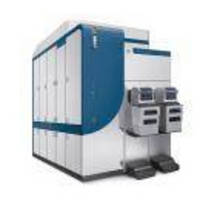
Wafer Inspection System finds defects in 22 nm devices.
Applied UVisionÃ-® 4 enables chipmakers to find defects in critical patterning layers of 22 nm and below logic/memory devices. Product combines DUV laser illumination, programmable polarization, and ultra-sensitive scattered light detectors to achieve optimal inspection sensitivity. Flexible optical system supports wide dynamic range detectors that allow all of chip to be imaged at once....
Read More »Semitool's New Raider-® Platform Used by Casio to Increase Lead-Free Capacity for 300mm Wafer-Level Packaging
Semitool Delivers Follow-on Raider for 300mm Lead-Free Electroplating KALISPELL, Mont., Dec. 5 -- Semitool, Inc. (NASDAQ:SMTL), a leading manufacturer of advanced single-wafer deposition and surface preparation process equipment for the semiconductor and wafer-level packaging industry, today announced the delivery of a follow-on order for Semitool's electroplating Raider tool by Japan-based Casio...
Read More »SEMITOOL Delivers Raider to Major North American IDM
Advanced Single-Wafer Cleaning Provides Leading-Edge FEOL and BEOL Processes - KALISPELL, Mont., Sept. 15 -- Semitool, Inc. (NASDAQ:SMTL), a leading manufacturer of wafer processing equipment for the semiconductor industry, today announced the delivery of a Raider SP cleaning system to a major North American fab. The system will be used for delivery of advanced front-end of line (FEOL) and...
Read More »Applied Materials and Singapore's Institute of Microelectronics to Set up Advanced Packaging Center
Singapore, Apr 13, 2011 - Applied Materials, Inc., the global leader in providing manufacturing solutions for the semiconductor, flat panel display and solar photovoltaic industries, today signed an agreement with the Institute of Microelectronics (IME), a world-renowned research institute under the Agency for Science, Technology and Research (A*STAR), to set up a Center of Excellence in Advanced...
Read More »
Dielectric Deposition System is designed for 3D chip packaging.
Applied ProducerÃ-® InVia(TM) dielectric deposition system uses CVD process to deposit uniform, thick oxide films in greater than 10:1 high aspect ratio (HAR) through-silicon via (TSV) structures. Process also enables electrical isolation of TSV to ensure reliable performance. For 3D packaging schemes, it electrically connects chips that are vertically stacked to boost speed and lower power...
Read More »
Wafer Inspection System finds defects in 22 nm devices.
Applied UVisionÃ-® 4 enables chipmakers to find defects in critical patterning layers of 22 nm and below logic/memory devices. Product combines DUV laser illumination, programmable polarization, and ultra-sensitive scattered light detectors to achieve optimal inspection sensitivity. Flexible optical system supports wide dynamic range detectors that allow all of chip to be imaged at once....
Read More »Applied Materials to Accelerate Its Solar Roadmap with Acquisition of Baccini
Applied Materials, Inc. today announced an agreement to acquire Baccini S.p.A., a leading supplier of automated metallization and test systems for manufacturing crystalline silicon (c-Si) photovoltaic (PV) cells. This integrated equipment set addresses critical processing steps in c-Si solar cell production that significantly affect solar cell efficiency and yield, while enabling the use of...
Read More »Applied Materials Named Green Energy Innovator of the Year
Applied Materials, Inc. today announced it was named Green Energy Innovator of the Year for its pioneering work on the Applied SunFab(TM) Thin Film Line, at a gala presenting the prestigious 9th Annual Platts Global Energy Awards. Applied Materials is focused on lowering the cost of solar photovoltaic generated energy through the application of nanomanufacturing technologies, said Mark Pinto,...
Read More »Applied Materials and Elpida Sign Major Service Agreement to Increase Fab Productivity
Applied certified customer engineers will work at Elpida's fabs using the latest diagnostic and monitoring techniques to provide preventive and corrective maintenance. We are pleased to be working more closely with the Applied Materials' service organization to drive down the cost of fab operations, said Mr. Jiro Yamamoto, Elpida officer and Hiroshima plant manager. As we expand our manufacturing...
Read More »Applied Materials Launches Strategy to Reduce the Cost Per Watt of Solar Power
SANTA CLARA, Calif.-- Sept. 5, 2006--Applied Materials, Inc. (NASDAQ:AMAT), the global leader in equipment and services for manufacturing semiconductors and flat panel displays, today launched its strategy to enter the rapidly growing solar photovoltaic (PV) equipment market. Applied Materials will provide a combination of manufacturing tools, together with technology and process innovations from...
Read More »EMC-3D Consortium Created for the Development of Cost-Effective 3D Thru-Silicon-Via Interconnect
SALZBURG, Austria, Oct. 11 /PRNewswire-FirstCall/ -- EMC-3D is a new consortium created to address the technical and cost issues of creating 3D interconnects using TSV technology for chip stacking and MEMS/sensors packaging. Several major equipment manufactures have joined with material companies to work with key research groups to address the issues of cost-effective manufacturing and...
Read More »Semitool's New Raider-® Platform Used by Casio to Increase Lead-Free Capacity for 300mm Wafer-Level Packaging
Semitool Delivers Follow-on Raider for 300mm Lead-Free Electroplating KALISPELL, Mont., Dec. 5 -- Semitool, Inc. (NASDAQ:SMTL), a leading manufacturer of advanced single-wafer deposition and surface preparation process equipment for the semiconductor and wafer-level packaging industry, today announced the delivery of a follow-on order for Semitool's electroplating Raider tool by Japan-based Casio...
Read More »SEMITOOL Delivers Raider to Major North American IDM
Advanced Single-Wafer Cleaning Provides Leading-Edge FEOL and BEOL Processes - KALISPELL, Mont., Sept. 15 -- Semitool, Inc. (NASDAQ:SMTL), a leading manufacturer of wafer processing equipment for the semiconductor industry, today announced the delivery of a Raider SP cleaning system to a major North American fab. The system will be used for delivery of advanced front-end of line (FEOL) and...
Read More »