

Rudolph Technologies, Inc.
PO Box 860
Budd Lake, NJ 07828
Share:
Rudolph's Discover Yield Management Software Gains Traction in Advanced Packaging Applications
Back-end manufacturers adopt front-end strategies to maximize yields with analysis of inspection and metrology data Flanders, New Jersey - Rudolph Technologies, Inc. (NASDAQ: RTEC), a leading provider of process characterization equipment and software for the semiconductor, FPD, LED and solar industries, announced today the sale of its DiscoverÃ-® Yield Management Software to a major...
Read More »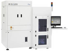
Rudolph Launches F30 Advanced Macro Inspection Module
High throughput, robust capability among key features driving new orders Flanders, New Jersey -Rudolph Technologies, Inc. (NASDAQ: RTEC), a leading provider of process characterization equipment and software for wafer fabs and advanced packaging facilities, today announced the global launch of the F30(TM) Advanced Macro Inspection Module, further extending the capabilities of the ExplorerÃ-®...
Read More »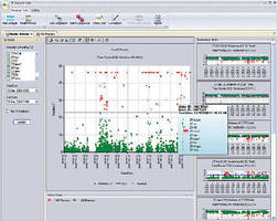
Software optimizes solar cell production.
Helping photovoltaic (PV) manufacturers increase cell efficiency, Discover Solar(TM) incorporates database structure and analysis engine optimized for unique requirements of high-volume production. Engineers can monitor health of complete production line, identifying tool and sub-component problems as well as incoming material issues. Fab management software tool offers statistical process...
Read More »Thin Film Metrology Tool suits DRAM metrology applications.
MetaPULSE IIIa(TM) makes film thickness measurements in aluminum-based DRAM manufacturing processes using picosecond ultrasonic laser sonar (PULSE(TM)) technology, which provides on-product thickness and material characterization for opaque films over range of types, dimensions, and multilayered configurations. Suited for fab-worthy measurements in DRAM and flash memory manufacturing process...
Read More »Multi-Surface Inspection System uses cluster architecture.
Offering full color, image-based inspection with real-time capture capability, Explorer(TM) Inspection Cluster uses adaptive wafer scheduling and offers flexible configurability. Individual systems can be configured with any combination of wafer backside and edge inspection capabilities to suit application. Designed for macro inspection, system is built on automated handling platform that...
Read More »Data Analysis Software provides yield management.
Offering comprehensive capture and analysis of process performance information, Discover(TM) Data Analysis System allows manufacturers to discover and act upon yield improvement opportunities. Defect classification and spatial pattern recognition minimize time spent reviewing known defects, while statistical process control with automated reporting and alerts gets critical information to correct...
Read More »Wafer Inspection System suits price-sensitive applications.
Automated macro defect inspection solution, NSXÃ-® 100, is designed for back-end manufacturing environment as well as front-end quality assurance (QA) applications. Able to handle wafers up to 200 mm at throughputs to 88 wph, system detects macro defects (0.5 micron and larger) to provide QA and feedback on process performance. Balance of throughput and resolution is suited to processes such...
Read More »Systems detect defects and correlate them to frontside die.
Inspection tool-set, comprised of NSX(TM) and B20(TM) Systems, features backside color processing capability and auto-die classification. NSX Systems offer frontside inspection, B20 Systems offer backside inspection, and Harmony ASR(TM) (all-surface review) Software offers defect analysis and management. Combined with brightfield and darkfield capabilities, B20 Systems use color processing...
Read More »Metrology System measures ultra thin films.
Combining PULSE Technology(TM) with MMXRF technology on single platform, Synergy MPX(TM) System measures ultra thin opaque films, such as ALD layers. PULSE Technology consists of picosecond ultrasonic laser sonar technique that provides non-contact, non-destructive opaque film measurements from 40 angstroms to 6 Ã-µm. Monochromatic source eliminates virtually all background radiation, while...
Read More »Inspection System targets critical edge defects.
Using multiple color cameras, concurrent color image capture, and intrinsic ADC, E25(TM) System detects and classifies defects based on size, morphology, color, and location. Algorithm creates defect-free surface model of edge and uses model to detect defects. System provides edge inspection for CMP, etch, clean, deposition, pre-RTP, and final QA processes, and is designed to cope with curved...
Read More »Rudolph Technologies Receives Orders for Over $15 Million from Major Memory Manufacturer
Process control systems used for advanced packaging of DRAM products in Korea and China facilities; additional orders expected to meet capacity ramp Wilmington, Mass. (January 15, 2019)—Rudolph Technologies, Inc. (NYSE: RTEC) announced today that it has received orders for over $15 million of legacy and new process control systems from a memory manufacturer based in Asia. The systems will be...
Read More »Rudolphâ™s Novusedge Selected by Leading Wafer Manufacturers for Bare Wafer Edge and Backside Inspection
Backlog for recently released system increases to over $12M Wilmington, Mass. (12/11/2018)—Rudolph Technologies, Inc. (NYSE: RTEC) today announced the receipt of over $12M in new orders for its recently-released NovusEdge™ system for edge and backside inspection on bare silicon wafers. The new orders are for capacity expansions at our existing customers as well as orders from two additional...
Read More »Rudolph Acquires Inspection Technology of Stella Alliance, LLC
Acquired patents to enhance Rudolph’s inspection capabilities in advanced packaging and extend inspection into new applications Flanders, New JerseyÃ- - Rudolph Technologies, Inc. (NYSE: RTEC) announced today that it has purchased Stella Alliance, LLC, a Massachusetts-based semiconductor inspection technology intellectual property (IP) portfolio company. Stella Alliance’s patented...
Read More »Rudolph's Discover Yield Management Software Gains Traction in Advanced Packaging Applications
Back-end manufacturers adopt front-end strategies to maximize yields with analysis of inspection and metrology data Flanders, New Jersey - Rudolph Technologies, Inc. (NASDAQ: RTEC), a leading provider of process characterization equipment and software for the semiconductor, FPD, LED and solar industries, announced today the sale of its DiscoverÃ-® Yield Management Software to a major...
Read More »
Rudolph Launches F30 Advanced Macro Inspection Module
High throughput, robust capability among key features driving new orders Flanders, New Jersey -Rudolph Technologies, Inc. (NASDAQ: RTEC), a leading provider of process characterization equipment and software for wafer fabs and advanced packaging facilities, today announced the global launch of the F30(TM) Advanced Macro Inspection Module, further extending the capabilities of the ExplorerÃ-®...
Read More »Rudolph Technologies, Inc. Analyst Event 2011 and Luncheon
MONDAY, FEBRUARY 7, 2011 MARRIOTT MARQUIS HOTEL / NEW YORK, NY WHAT: The management of Rudolph Technologies, Inc. (Nasdaq: RTEC), Paul McLaughlin, Chairman & Chief Executive Officer, and Steven Roth, Chief Financial Officer, cordially invites the professional investment and finance communities and the industry media to the Company's 2011 Analyst Event, to be held Monday, February 7, in New York...
Read More »Rudolph Technologies Appoints Avishai Kepten as Vice President and General Manager
Flanders, New Jersey (October 21, 2010) - Rudolph Technologies, Inc. (Nasdaq: RTEC), a leading provider of process characterization equipment and software for wafer fabs and advanced packaging facilities, today announced the appointment of Dr. Avishai Kepten as Vice President and General Manager of the Company's Metrology Business Unit. Dr. Kepten has over 25 years of experience in the...
Read More »Rudolph Technologies Appoints STAr Technologies as Authorized Vendor for Probe Card Interfaces in Asia
Appointment provides customers in region with a cost-effective, local supplier for probe card interfaces Flanders, New Jersey (Sept. 7, 2010)-Rudolph Technologies, Inc. (NASDAQ: RTEC), a leading provider of process characterization equipment and software for wafer fabs and advanced packaging facilities, announces that it has signed an agreement with STAr Technologies to be an authorized...
Read More »
Software optimizes solar cell production.
Helping photovoltaic (PV) manufacturers increase cell efficiency, Discover Solar(TM) incorporates database structure and analysis engine optimized for unique requirements of high-volume production. Engineers can monitor health of complete production line, identifying tool and sub-component problems as well as incoming material issues. Fab management software tool offers statistical process...
Read More »Rudolph Joins Leading Chipmakers in SEMATECH's Metrology Program at UAlbany NanoCollege
Joint creation of International Process Characterization program will integrate inspection, metrology and data analysis solutions to enable manufacturing at 32 nm and beyond FLANDERS, NJ and ALBANY, NY (February 20, 2008)-Rudolph Technologies, Inc. (NASDAQ: RTEC), a leading provider of process characterization equipment and software for thin film measurement and macro defect inspection, and...
Read More »