

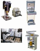
Owens Design, Inc.

Fremont, CA 94538


Wafer Flip Module enables backside contamination inspection.
Designed for 300 and 200 mm wafers, Wafer Flip Module is compatible with edge grip and vacuum paddle end effectors. It has 2 motors, one for flipping and one for wafer gripper mechanism. Rotation of 180Ã-
Read More »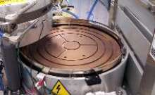
Heating/Cooling System handles 200 and 300 mm wafers.
Heating/Cooling Module is BOLTS compatible for integration with standard wafer handling automation. It uses resistive heating elements to achieve better than 450Ã-
Read More »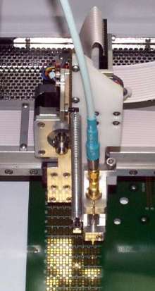
Robotic Probers target semiconductor test industry.
Robotic Probers provide method for validating and calibrating automatic test equipment. Robots attach directly to test head and probe specific pads on device interface board. On-board CPU commands probe tip to move along high-precision linear bearings using optically encoded stepper motors for accurate positioning.
Read More »Owens Design's Solar Equipment Design and Manufacturing Business Grows 152 Percent in Last Year
Collaborative Tool Design Enables Technology Leadership by Reducing Risk, Time, and Cost in Deploying New Process Technologies. FREMONT, Calif., Oct. 6 - Owens Design Inc. - a leading design and manufacturing partner for the solar, semiconductor, and data storage industries today announced that bookings from new tool design and manufacturing contracts with companies in the solar market have...
Read More »
Wafer Flip Module enables backside contamination inspection.
Designed for 300 and 200 mm wafers, Wafer Flip Module is compatible with edge grip and vacuum paddle end effectors. It has 2 motors, one for flipping and one for wafer gripper mechanism. Rotation of 180Ã-
Read More »Owens Design Expands To Larger Facilities
FREMONT, CA - Owens Design Inc., a provider of turnkey design and manufacturing services for complex capital equipment, announced that due to continued growth it is moving to larger facilities. The new facilities feature expanded design, manufacturing, and cleanroom space. Within a short distance of the current location, the Company's new address will be 47427 Fremont Blvd. All phone numbers and...
Read More »
Heating/Cooling System handles 200 and 300 mm wafers.
Heating/Cooling Module is BOLTS compatible for integration with standard wafer handling automation. It uses resistive heating elements to achieve better than 450Ã-
Read More »
Robotic Probers target semiconductor test industry.
Robotic Probers provide method for validating and calibrating automatic test equipment. Robots attach directly to test head and probe specific pads on device interface board. On-board CPU commands probe tip to move along high-precision linear bearings using optically encoded stepper motors for accurate positioning.
Read More »