

Canon USA, Inc.
Melville, NY 11747
Share:
Compact HD Camera suits live broadcasts, production, surveillance.
Modular multipurpose 8.2 MP Super 35 mm box camera, Model ME200S-SH,Ã- employs Dual Pixel CMOS autofocus (DAF) technology, which provides focusing options when using Canon EF lenses and CINE-SERVO lenses. Along with remote manual control of focus, iris, auto exposure (AE) and ND filters with optional Canon RC-V100 controller, features include 1920x1080 / 60p, 50p output, IR shooting...
Read More »Canon U.S.A.'s Teleretinal Solutions on Display at Vision Expo East
MELVILLE, N.Y. - In today's healthcare environment, it is essential to invest in solutions that help streamline workflows while having features that can assist eye care professionals with their compliance efforts. Canon U.S.A., Inc., a leader in digital imaging solutions, will showcase solutions designed to address these needs during this year's Vision Expo East convention at the Jacob Javits...
Read More »Green Bay Blue Scores with the Océ ColorWave 600 Printer
Reprographic Shop Creates Eye-Catching Banners in Record Time to Welcome Home Football Champs Trumbull, CT - Green Bay, Wisconsin-based reprographer Green Bay Blue knows that having the right equipment at your fingertips is crucial to delivering high-quality work, especially in fast turnaround time situations. In fact, the shop's recent investment in an OcÃ-© ColorWaveÃ-® 600 large format...
Read More »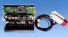
Motor Encoder offers scanning speed of 60 Hz.
Model FS1 consists of laser diffraction and interference rotary encoder with single-phase, 4-pole coreless, brushless dc motor and dedicated controller. Compatible with high-speed raster scanning systems with large diameter beams, encoder is suited for applications in rapid-prototyping and PC board manufacturing. It offers scan angle of Ã-
Read More »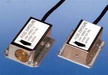
Micro Laser Interferometer fits in tight spaces.
Combining Michelson interferometer with 650 nm semiconductor laser in 47 x 32 x 19 mm package, Model DS-80 provides continuous detection of tiny movements in variety of products and applications. Non-contact displacement sensor is capable of 0.08 nm resolution with response of 50 Hz. Measuring range is Ã-
Read More »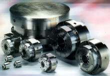
Air Bearing offers minimized air flow.
Made of porous carbon material, AB Series minimizes air flow and friction and is suited for head testing and media certification applications. Model AB-36RV has axial load of 4.2-5.0 Kgf, radial load from 3.8-5.0 Kgf, and radial and axial stiffness of 2.5 Kgf and 2.8 Kgf/Ã-µm respectively. Model AB-50RV model features axial load from 7.2-9.0 Kfg, radial load from 5.0-6.3 Kgf, and radial and...
Read More »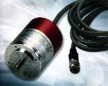
Laser Rotary Encoder withstands factory environments.
Measuring 56 mm, heavy-duty Model M1-H features max frequency response of 8.3 MHz and max rotation rate of 10,000 rpm. Balanced line driver output circuit allows for long distance signal transmissions. System's 780 mm semiconductor laser offers max output power of 5 mW, with signal error of 25 arc-sec. Encoder is suited for computer/electronics, imaging systems, optical scanners, semiconductor...
Read More »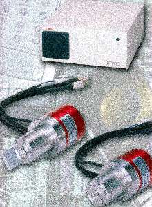
Encoder System suits portable, electronic devices.
Model KP-1SM100 is based on laser rotary encoder technology. It obtains significant temperature characteristics by employing digital servo controllers and encoders with diffraction interference systems that utilize diffraction of laser beams. Scanning angle is -±10-° and rotor inertia is 10.5 gcm-sq with 30 mm diameter mirror, resulting in positioning resolution of .02 arc sec. System can be...
Read More »Canon U.S.A. Receives ENERGY STAR-® Partner of the Year - Sustained Excellence Award for 2021
This Prestigious Honor Signifies the Company's Ongoing Commitment to Environmental Sustainability through the use of Energy-Efficient Technologies in a Variety of Products Melville, N.Y., April 13, 2021 /PRNewswire/ -- Canon U.S.A., Inc., a leader in digital imaging solutions, announced today that it is the proud recipient of the 2021 ENERGY STAR® Partner of the Year Award for Sustained...
Read More »Canon Inc. Makes Carbon Disclosure Project's (CDP) 'A-List' in Two Categories
MELVILLE, N.Y., Dec. 17, 2020 /PRNewswire/ -- Canon U.S.A., Inc. today announced that its parent company, Canon Inc.,'s environmental initiatives have been recognized by the international environmental non-profit organization Carbon Disclosure Project (CDP)(1), based in the United Kingdom, in the fields of climate change and water security, and awarded a spot on the CDP's A-List in both...
Read More »Canon U.S.A. Awarded Energy Star-® Partner of the Year - Sustained Excellence Award for 2020
This Prestigious Award Signifies the Company's Ongoing Commitment to Environmental Sustainability through use of Energy-Efficient Technologies in a Range of Products MELVILLE, N.Y., April 2, 2020 /PRNewswire/ -- Canon U.S.A. Inc., a leader in digital imaging solutions, is proud to announce it has been awarded the 2020 ENERGY STAR® Partner of the Year award for Sustained Excellence for the...
Read More »Canon Medical Completes Acquisition of Toshibaâ™s Imaging Systems Division
Toshiba Imaging Systems will formally become a Canon Medical entity called Video Sensing Division Tustin, Calif. – Oct. 1, 2019 – The Video Sensing Division of Canon Medical Systems USA, Inc. (Tustin, CA - www.us.medical.canon/VSD), today announced that Canon Medical will complete its acquisition of the Video Sensing Division (VSD), formerly known as TAIS’ Imaging Systems Division (ISD),...
Read More »Canon, HP Take Home First-Ever BLI PaceSetter Awards for Leadership in MFP Accessibility
FAIRFIELD, N.J. (PRWEB) MAY 22, 2019 Keypoint Intelligence - Buyers Lab (BLI), the world’s leading independent evaluator of document imaging software, hardware, and services, today announced the winners of its BLI PaceSetter awards in the MFP Accessibility arena. This award recognizes the document imaging OEMs that offer the strongest set of accessibility features in their MFPs, while also...
Read More »Canon Central and North Africa Partners with Yaba College of Technology in Nigeria to Develop Student Talent for Careers in the Printing Industry in Africa
Canon will be holding print training for students at Yaba College of Technology which is Nigeria’s first higher institution to have established a Centre for Entrepreneurship Development LAGOS, Nigeria, April 1, 2019/ -- Canon Central and North Africa (CCNA) (www.Canon-CNA.com) a leader in imaging solutions, has signed a 3 year partnership agreement with Yaba College of Technology (Yabatech)...
Read More »Canon Takes Home Buyers Lab PaceSetter Award for Outstanding Serviceability in the United States
Keypoint Intelligence - Buyers Lab (BLI) today announced that Canon U.S.A, Inc., is the winner of the BLI PaceSetter award for Outstanding Serviceability 2018–2019. FAIRFIELD, N.J. (PRWEB) SEPTEMBER 04, 2018 - Keypoint Intelligence - Buyers Lab (BLI), the world’s leading independent evaluator of document imaging software, hardware and services, today announced that Canon U.S.A, Inc., is the...
Read More »Canon Celebrates the Global Success of Océ CrystalPoint Technology
10,000 Océ ColorWave Engines Powered with this Technology Now Installed Worldwide MELVILLE, N.Y., Feb. 7, 2018 - Canon Solutions America, Inc., a wholly owned subsidiary of Canon U.S.A., Inc., Canon U.S.A., Inc. a leader in digital imaging solutions, is proud to announce an important milestone for its long heralded Océ CrystalPoint® technology: 10,000 Océ ColorWave engines, powered by this...
Read More »Canon Wins BLIâ™s 2018 Copier MFP Line of the Year
For the third year in a row, Canon is the winner of the Keypoint Intelligence - Buyers Lab (BLI) Copier MFP Line of the Year. FAIRFIELD, N.J. (PRWEB) JANUARY 24, 2018 For the third year in a row, Canon is the winner of the Keypoint Intelligence - Buyers Lab (BLI) Copier MFP Line of the Year. BLI, the world’s leading authority on document imaging devices and software solutions, presents its...
Read More »Compact HD Camera suits live broadcasts, production, surveillance.
Modular multipurpose 8.2 MP Super 35 mm box camera, Model ME200S-SH,Ã- employs Dual Pixel CMOS autofocus (DAF) technology, which provides focusing options when using Canon EF lenses and CINE-SERVO lenses. Along with remote manual control of focus, iris, auto exposure (AE) and ND filters with optional Canon RC-V100 controller, features include 1920x1080 / 60p, 50p output, IR shooting...
Read More »