FEI Co.
Hillsboro, OR 97124
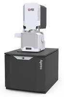
Scanning Electron Microscope supports diverse applications.
With compound final lens, Apreo™Ã- offers resolution down to 1.0 nm at 1 kV, without need for beam deceleration, for optimal performance on sampleÃ- even if it is tilted or topographic. Backscatter detection is offered at lowest beam currents, at any tilt angle, on sensitive samples, and at TV-rate imaging to maximize materials contrast, and detector segments can be individually...
Read More »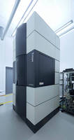
FEI and CEOS Deliver First Sub-Angstrom, Low-Voltage Electron (SALVE) Microscope to the University of Ulm
Developed in the frame of University Ulm's SALVE project, the microscope provides high-contrast, atomic-scale imaging of radiation-sensitive samples, such as graphene and organic materials. Hillsboro, Ore. and Heidelberg, Germany — FEI (NASDAQ: FEIC) and CEOS announced today that they have delivered the first sub-Ãâ¦ngstrom, low-voltage electron (SALVE) microscope to the University of...
Read More »FEI and Oregon Health and Science University Install a Complete Correlative Microscopy Workflow in Newly Built Collaborative Science Facility
Installation is part of an expansion of the OHSU/FEI Living Lab for Cell Biology collaboration; a complete correlative microscopy solution will enable new approaches for cancer and related disease research Portland, Ore. –Ã- FEI (NASDAQ: FEIC) and Oregon Health and Science University (OHSU) today announced an expansion of their Living Lab for Cell Biology agreement that includes the...
Read More »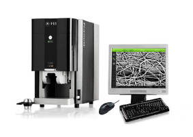
Automated System measures micro- and nano-fibers.
Powered by Phenom(TM) personal electron microscope, Fibermetric(TM) System discovers and quantifies properties of woven and nonwoven fiber samples in minutes. System automatically collects hundreds of measurements per image, and generates fiber and pore size distribution plots for quality control and for predicting application properties such as filtration efficiency. Magnifications up to 24,000...
Read More »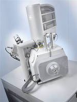
SEM can be used with wide range of samples.
With ability to scan variety of samples, including insulated, wet, and dirty samples, Quanta 50 Series scanning electron microscope can be utilized in materials research, mineralogy, chemicals and petroleum, electronics, pharmaceuticals, and biology industries. Beam deceleration optimizes surface imaging capability with low landing energies, while SmartSCAN(TM) technology minimizes noise. Quanta...
Read More »Cryogenic Freezing Tool features touchscreen user interface.
Vitrobot Mark IV cryo sample preparation tool physically fixates biological structures within ultrathin vitrified ice layers so samples can withstand high voltages such as those used in 3-dimensional transmission electron microscopy. Features include Linux operated touchscreen interface and robotics, and automated vitrification medium to liquid nitrogen atmosphere transfer.
Read More »Software System provides SEM and EDS validation.
Suited for forensics and mining applications, microValidator(TM) provides automatic, standards-based confirmation of imaging and analytical performance that is critical in establishing accuracy, traceability, and reproducibility of results. Package includes software, beam current meter, and sub-stage mount containing essential standards. Offering SEM, EDS, and combined SEM/EDS checks, system...
Read More »Microscope bridges optical and scanning electron microscopy.
Facilitating operation via interactive touchscreen, Phenom(TM) can be used in most locations and does not require specialized facilities. Solution yields magnification up to 20,000x in compact design to bring high-resolution imaging to industrial as well as academic applications. Example areas of use include quality assurance, product development, research, and teaching.
Read More »High Resolution Microscope magnifies up to 20,000x.
Phenom(TM) high-resolution imaging microscope features performance levels between those of optical and scanning electron microscopes. Capable of yielding magnification up to 20,000x, unit features interactive touch screen user interface. Suitable applications include quality assurance, product development, research, and teaching. Unit is portable and requires no specialized facilities.
Read More »
Circuit Edit/Validation System uses ion column technology.
Offering circuit edit capabilities, V600CE accelerates semiconductor design validation and performance optimization on 65 nm and below devices. Etching planarity is promoted with NanoChemix(TM) tri-nozzle gas delivery system, which accommodates range of precursors for etching and deposition. Dynamic end-point solution displays live imaging of active pattern as well as both stage current readings...
Read More »
Scanning Electron Microscope supports diverse applications.
With compound final lens, Apreo™Ã- offers resolution down to 1.0 nm at 1 kV, without need for beam deceleration, for optimal performance on sampleÃ- even if it is tilted or topographic. Backscatter detection is offered at lowest beam currents, at any tilt angle, on sensitive samples, and at TV-rate imaging to maximize materials contrast, and detector segments can be individually...
Read More »
FEI and CEOS Deliver First Sub-Angstrom, Low-Voltage Electron (SALVE) Microscope to the University of Ulm
Developed in the frame of University Ulm's SALVE project, the microscope provides high-contrast, atomic-scale imaging of radiation-sensitive samples, such as graphene and organic materials. Hillsboro, Ore. and Heidelberg, Germany — FEI (NASDAQ: FEIC) and CEOS announced today that they have delivered the first sub-Ãâ¦ngstrom, low-voltage electron (SALVE) microscope to the University of...
Read More »FEI Announces Agreement to Acquire DCG Systems
Expansion of Workflow Offerings to Semiconductor Customers HILLSBORO, Ore. –Ã- FEI Company (NASDAQ: FEIC) and DCG Systems, Inc. today announced a definitive agreement under which FEI would acquire DCG for $160 million in an all cash transaction. DCG is a leading supplier of electrical fault characterization, localization and editing equipment, serving process development, yield ramp and...
Read More »FEI and Oregon Health and Science University Install a Complete Correlative Microscopy Workflow in Newly Built Collaborative Science Facility
Installation is part of an expansion of the OHSU/FEI Living Lab for Cell Biology collaboration; a complete correlative microscopy solution will enable new approaches for cancer and related disease research Portland, Ore. –Ã- FEI (NASDAQ: FEIC) and Oregon Health and Science University (OHSU) today announced an expansion of their Living Lab for Cell Biology agreement that includes the...
Read More »FEI Launches New Website for Natural Resources
Website is part of a new business focus on the mining, oil & gas, and geosciences industries Brisbane, Australia, November 15, 2010―FEI Company (NASDAQ: FEIC), has launched a website for natural resources as part of an increased focus on the mining and oil & gas industries. The website will serve as a technical and educational resource regarding FEI solutions, such as automated mineralogy, for...
Read More »FEI Releases New Guide to Electron Microscopy
Get a view into the world of nanotechnology through this all-new edition of FEIs industry-leading An Introduction to Electron Microscopy Hillsboro, Ore./October 14, 2010 - FEI Company (NASDAQ: FEIC), a leading instrumentation company providing electron microscope systems for applications across many industries, announces the availability of An Introduction to Electron Microscopy, an all-new...
Read More »
Automated System measures micro- and nano-fibers.
Powered by Phenom(TM) personal electron microscope, Fibermetric(TM) System discovers and quantifies properties of woven and nonwoven fiber samples in minutes. System automatically collects hundreds of measurements per image, and generates fiber and pore size distribution plots for quality control and for predicting application properties such as filtration efficiency. Magnifications up to 24,000...
Read More »
SEM can be used with wide range of samples.
With ability to scan variety of samples, including insulated, wet, and dirty samples, Quanta 50 Series scanning electron microscope can be utilized in materials research, mineralogy, chemicals and petroleum, electronics, pharmaceuticals, and biology industries. Beam deceleration optimizes surface imaging capability with low landing energies, while SmartSCAN(TM) technology minimizes noise. Quanta...
Read More »FEI Opens China NanoPort
New Facility to Focus on Collaboration with Researchers and Developers HILLSBORO, Ore./January 18, 2008 - FEI Company (Nasdaq: FEIC) today opened a NanoPort in Shanghai, China. The new facility is the fourth such location joining those already in operation in North America, Europe and Japan. FEI NanoPorts go beyond being mere demo centers. They provide centers of technical and applications...
Read More »FEI Introduces FEI.com for Owners Featuring FEI Connect
New Service Enables Online Networking and Sharing of Application Expertise and Best Practices SEPTEMBER 24, 2007/Hillsboro, Ore.-FEI Company (Nasdaq: FEIC) has introduced a new and exclusive service for its customers that will enable its prestigious global base of electron microscopy users to collaborate online as a professional community. The service further extends FEI's leadership as a...
Read More »


