Wafer Coating Process is hosted on mass imaging platform.
Share:
Press Release Summary:
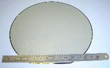
Capable of exceeding ±12.5 mm Total Thickness Variation stipulated by wafer processing specialists, backside wafer coating process is compatible with underfill or adhesive-type coatings normally applied at nominal 50 mm thickness to backside of semiconductor wafers ahead of singulation. Process is also compatible with metal stencil and emulsion screen technologies, which enable materials with larger filler particles to be applied with smooth surface finish.
Original Press Release:
Mass Imaging Speed and Cost Advantages Penetrate Backside Wafer Processing
DEK has successfully developed a high throughput backside wafer coating process, hosted on a cost-effective mass imaging platform and capable of exceeding the ± 12.5 mm Total Thickness Variation (TTV) stipulated by most wafer processing specialists. The new process is compatible with underfill or adhesive-type coatings, normally applied at a nominal 50 mm thickness to the backside of semiconductor wafers ahead of singulation.
"TTV is the critical success factor for any backside wafer coating process," said Clive Ashmore of DEK's global applied process engineering group. "By demonstrating our ability to meet the established criteria for backside wafer processing, we have opened new opportunities for semiconductor packaging specialists to increase throughput and reduce the cost per package by using high accuracy mass imaging. The equipment used is also inherently more flexible than dedicated backside coating machines, delivering an even higher return on investment for our customers."
The new process is compatible with DEK's metal stencil and emulsion screen technologies. Metal stencils enable materials with larger filler particles, such as encapsulation materials to be applied with a totally smooth surface finish. Mesh stencils allow other materials such as thermoplastic adhesives to be deposited accurately and at high speed. In each case, the capabilities of both the machine and the stencil technology to achieving control over the print thickness and ensuring uniformity at high production volumes.
"To develop backside wafer coating as a turnkey process, ready for our customers to use immediately, our global applied process engineers are able to deliver a full implementation service at customer sites world-wide," added Ashmore. "We are now intimately familiar with the impact of stencil technology, thread size, emulsion thickness, metal thickness, squeegee or ProFlow selection, and machine parameter settings, when implementing backside wafer processing using high accuracy mass imaging techniques."
About DEK
DEK is a global provider of advanced pre-placement manufacturing solutions and innovative deposition technologies for a wide range of electronic materials. For more information, visit DEK at www.dek.com.
Company Contact Agency Contact
Rich Heimsch
DEK International GmbH.
Geroldstrasse 28
4 Stock
Ch-8005 Zurich
Switzerland
Tel: +41 1 274 80 20
Fax: +41 1 274 80 22
E-mail: rheimsch@dek.com
Internet: www.dek.com
Zoe Walter
Protean Marketing Communications Ltd
Communications House
Station Road
Cookham Rise
Maidenhead
Berkshire SL6 9BU
Tel: +44 1628 648530
Fax: +44 1628 529087
Email: zoe.walter@protean.co.uk
Internet: www.protean.co.uk