Thin Film Research Tool measures thickness and composition.
Share:
Press Release Summary:
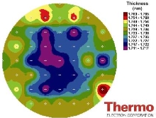 Utilizing parallel angle, resolved X-ray photoelectron spectroscopy technique, Theta 300 manages transition of new gate dielectrics and other thin structures from development into production. Fully automated unit features twin load ports and full host integration and pattern recognition. It provides 200 and 300 mm wafer mapping of thickness, elemental and chemical uniformity, coupled with non-destructive depth profiling to determine interface chemistry.
Original Press Release:
Thermo Electron Introduces Theta 300XT, 300mm Thickness and Composition Metrology for Ultra-thin Films and Shallow Implant
EAST GRINSTEAD, England (May 16, 2005) - Thermo Electron Corporation (NYSE:TMO) has evolved its Theta 300 thin film research tool to manage the transition of new gate dielectrics and other thin structures from development into production. Thermo's patented parallel angle resolved X-ray photoelectron spectroscopy technique produces accurate and repeatable measurement of thickness and composition in ultra-thin structures.
The new fully automated Theta 300XT tool features twin loadports and full host integration and pattern recognition for measurement of product wafers. Theta 300XT features 200mm and 300mm wafer mapping of thickness, elemental and chemical uniformity, coupled with non-destructive depth profiling to determine interface chemistry. This unique capability allows a metrology of thickness and composition that relates directly to device electrical performance.
With the development of this new "at-line" tool, Thermo is supporting the current and future needs of the Semiconductor and Nanotech industries as they introduce novel materials and ultra-thin structures. Semiconductor device speed can no longer be improved by simple scaling. Engineers and scientists have used the Theta 300 research tool to develop processes with new gate dielectrics, barrier metals, and shallow implants. These processes are now entering production, and Thermo's unique measurement capability is required on product wafers with greater throughput and precision. Theta 300XT addresses this need.
For more information about the Theta 300XT, please call +1 800-532-4752, e-mail analyze@thermo.com or visit www.thermo.com/surfaceanalysis
About Surface Analysis
Thermo Electron Corporation manufactures a range of instruments for surface, ultra-thin film and thin film analysis. We supply systems for X-ray Photoelectron Spectroscopy (XPS), Auger Electron Spectroscopy (AES) and multi-technique instruments. ESCALAB 250 is a high-performance, multi-technique XPS instrument, THETA PROBE is a small-spot XPS instrument capable of producing angle-resolved XPS data without tilting the sample, THETA 300 provides data from semiconductor wafers and MICROLAB 350 is a high-performance scanning Auger spectrometer. In addition to complete systems, we manufacture surface analysis components for techniques such as XPS, ARXPS, AES, SAM, UPS and ISS. For more information visit www.thermo.com/surfaceanalysis
About Thermo Electron Corporation
Thermo Electron Corporation is the world leader in analytical instruments. Our instrument solutions enable our customers to make the world a healthier, cleaner and safer place. Thermo's Life and Laboratory Sciences segment provides analytical instruments, scientific equipment, services and software solutions for life science, drug discovery, clinical, environmental and industrial laboratories. Thermo's Measurement and Control segment is dedicated to providing analytical instruments used in a variety of manufacturing processes and in-the-field applications, including those associated with safety and homeland security. Based near Boston, Massachusetts, Thermo has revenues of more than $2 billion, and employs approximately 10,000 people in 30 countries. For more information, visit www.thermo.com.