Optical Image Stabilization IC targets smartphone cameras.
Share:
Press Release Summary:
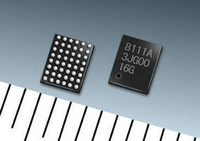
Supplied in 2.57 x 3.22 x 0.69 mm lead-free/halogen-free package, Model LC898111AXB-MH combines controller and driver functionality, enabling precise suppression control of camera shaking and allowing implementation of pan/tilt function for walk-and-take situations. IC also includes 2-channel position sensing circuit, gyro-filter interface circuit, and lens-server circuit. Output of integrated PWM driver minimizes power consumption as well as effects of noise on image quality.
Original Press Release:
ON Semiconductor Introduces Advanced Optical Image Stabilization Solution for Smartphone Camera Modules
Highly integrated OIS IC provides industry-leading low power solution for precise suppression control of camera shaking and remarkably effective pan and tilt functions
PHOENIX, Ariz. — ON Semiconductor (Nasdaq: ONNN), driving energy efficient innovations, has introduced the industry’s highest resolution optical image stabilization (OIS) integrated circuit (IC) for use in smartphone camera modules. This highly integrated LC898111AXB-MH solution delivers industry-leading accuracy and low power operation in a compact size.
The LC898111AXB-MH combines both the controller and driver functionality necessary for dealing with OIS in the camera modules incorporated into smartphone handsets. A significantly increased shutter speed leads to exposure compensation that is far superior to competing OIS solutions. As such, it enables precise suppression control of camera shaking to be achieved. Furthermore it allows implementation of Pan/Tilt function indispensable for walk-and-take situations. The output of the IC’s integrated pulse width modulated (PWM) driver lowers power consumption as well as reduces the effect of noise on image quality. This highly-integrated, program-ready IC enables engineers to minimize the number of external components necessary in the system design - thereby reducing overall power consumption and board real estate utilization.
"There is growing demand for enhanced camera performance in the latest smartphone models, as consumers expect to derive better and better user experiences,” said Tomofumi Watanabe, business unit Leader of the Power Solutions Products in Intelligent Power Solution Division at ON Semiconductor. “Handset manufacturers need to specify higher resolution CMOS image sensors that are supported by greater degrees of OIS accuracy. This compact, highly-sophisticated, power efficient, single-chip solution helps in the design of smartphones which are lighter and sleeker while still being more feature-rich. The innovative LC898111AXB-MH IC has already been adopted by leading smartphone manufacturers and is currently in use in the highest resolution smartphone camera on the market today.”
The LC898111AXB-MH has numerous built-in digital and analog signal processing mechanisms. These include a two-channel position sensing circuit, a gyro-filter interface circuit and lens-servo circuit. The position sensing circuit contains a hall-amp circuit, constant current digital-to-analog converter (DAC), gain control operational amplifier and 12-bit analog-to-digital converters (ADCs) for each channel. The gyro-filter interface circuit is fully compatible in both analog and digital signals. Both the gyro-filter interface and lens-servo circuits are adjustable through the I2C and SPI bus interfaces, allowing comprehensive configuration when connecting with various gyros and actuators. As a result, the device can cover a wider shaking frequency range and thus offers a more expansive image stabilization angle.
Further expansion of the series is planned with the development of the LC898119XC-MH which offers the industry’s smallest chip size measuring 2.0mm X 2.0mm X 0.675mm, while providing extremely low power consumption; samples are available now.
Packaging and Pricing
The LC898111AXB-MH is offered in a compact (2.57 mm x 3.22 mm x 0.69 mm), lead-free/halogen-free P48-pin WLP package. It is priced at $2.3 USD per unit in 4,000 unit quantities.
About ON Semiconductor
ON Semiconductor (Nasdaq: ONNN) is driving energy efficient innovations, empowering design engineers to reduce global energy use. The company offers a comprehensive portfolio of energy efficient power and signal management, logic, discrete and custom solutions to help customers solve their unique design challenges in automotive, communications, computing, consumer, industrial, LED lighting, medical, military/aerospace and power supply applications. ON Semiconductor operates a responsive, reliable, world-class supply chain and quality program, and a network of manufacturing facilities, sales offices and design centers in key markets throughout North America, Europe, and the Asia Pacific regions. For more information, visit http://www.onsemi.com.
Follow @onsemi on Twitter.
ON Semiconductor and the ON Semiconductor logo are registered trademarks of Semiconductor Components Industries, LLC. All other brand and product names appearing in this document are registered trademarks or trademarks of their respective holders. Although the company references its Web site in this news release, such information on the Web site is not to be incorporated herein.
Contacts
Katsuya Ito
Media Relations – Japan
ON SemiconductorÂ
+81-(276) 61-8506
Katsuya.Ito@onsemi.com