Nano Indenter G200 features tip and sample heater.
Press Release Summary:
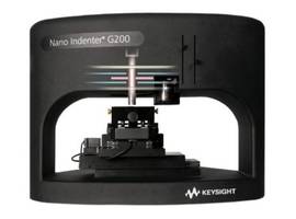
Measuring nanomechanical properties, Nano Indenter G200 uses high-power diode laser to heat the tip. Designed to purge samples with various gases, unit’s tip and sample heater support RT up to 500 °C temperature range. Equipped with substrate holder, product comes with transparent plate and built-in thermocouple. Indenter is embedded with dual-loop PID controller’s NanoSuite interface.
Original Press Release:
Keysight Technologies Introduces Nano Indenter G200 High-Accuracy Tip, Sample Heater - Measures Nanomechanical Properties at Precisely Controlled Temperatures, Minimizes Drift
Capability gives scientists and engineers many new and intriguing approaches for dynamic materials testing
Highlights:
- Fast heating allows dynamic nanoindentation and creep measurement
- Thermocoupled heated tip enables thermal equilibrium
- Adjustable laser spot size minimized heat-generating area, reducing thermal drift
Keysight Technologies, Inc. (NYSE: KEYS) today announced the availability of a high-accuracy tip and sample heater to expand the utility of its popular Nano Indenter G200. This easy-to-use solution uses a precise high-power diode laser to heat the sample and the indenter tip.
Benefits include the ability to measure nanomechanical properties at precisely controlled temperatures and to test a wide range of samples under highly dynamic temperature conditions. To ensure reliable data, the system minimizes drift associated with heating by using function-optimized materials and an adjustable laser spot size. Keysight Nano Indenter G200 users also have the option to purge samples with various gases to avoid contamination and oxidation.
The new tip and sample heater for the G200 supports a wide temperature range (RT up to 500 C) and is accurate to within 0.1 C. Another advantage is the high rate of the system’s heating and cooling processes. Depending on the temperature, the rate can exceed 20 K/sec in either direction. This capability affords scientists and engineers many new and intriguing opportunities for dynamic materials testing.
Keysight’s laser-heated indenter tip, a critical component of the new system solution, prevents disturbance of the substrate temperature during measurement. This stability is critical for working with materials that have poor thermal conductivity and whose mechanical properties are strongly affected by temperature. Keeping the tip and sample at the same temperature as one another also allows G200 users to perform high-temperature continuous stiffness measurements with exceptional precision.
The Nano Indenter G200 system’s substrate holder is optimized to provide the highest mechanical and temperature stability. To ensure simple and convenient G200 operation, the transparent plate underneath the sample contains a built-in thermocouple. When the absolute highest accuracy is needed, such as for nanoindentation applications involving thick polymer samples, users can mount a thermocouple to the sample surface. The dual-loop PID controller’s NanoSuite interface offers complete NanoSuite software integration.
Additional Information
More information about the Nano Indenter G200 is available at www.keysight.com/find/nanoindenter. Additional information about the U9820A-061 Laser Heater is available at www.keysight.com/find/G200-laserheater.
About Keysight in Nanomechanical Systems
Keysight Technologies offers high-precision, modular nanomeasurement solutions for research, industry and education. Exceptional worldwide support is provided by experienced application scientists and technical service personnel. Keysight’s leading-edge R&D laboratories ensure the continued, timely introduction and optimization of innovative, easy-to-use nanomechanical system technologies.
About Keysight Technologies
Keysight Technologies is a leading technology company that helps its engineering, enterprise and service provider customers optimize networks and bring electronic products to market faster and at a lower cost. Keysight’s solutions go where the electronic signal goes, from design simulation, to prototype validation, to manufacturing test, to optimization in networks and cloud environments. Customers span the worldwide communications ecosystem, aerospace and defense, automotive, energy, semiconductor and general electronics end markets. Keysight generated revenues of $2.9B in fiscal year 2016. In April 2017, Keysight acquired Ixia, a leader in network test, visibility, and security. More information is available at www.keysight.com.
Additional information about Keysight Technologies is available in the newsroom at www.keysight.com/go/news
CONTACTS:
Geri Lynne LaCombe
Americas +1 303 662 4748
Sarah Calnan
Europe +44 (118) 927 5101
Connie Wong
Asia +852 3197-7818