NAND Flash Memory Chips target embedded applications.
Press Release Summary:
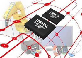
Available in 6 x 8 mm WSON and 10.3 x 7.5 mm SOP packages, Serial Interface NAND Series consists of 12 products with voltage ratings of 3.3 V or 1.8 V and densities of 1, 2, and 4 Gb. Devices include high-speed sequential read function, embedded ECC with bit flip count report function, and data protection features that can protect specific blocks. Typical embedded applications include flat screen TVs, printers, wearable devices, and robots.
Original Press Release:
Toshiba Debuts NAND Flash Memory Products for Embedded Applications
Compatible with Serial Peripheral Interface
IRVINE, Calif., – Toshiba America Electronic Components, Inc. (TAEC)*, a committed leader that collaborates with technology companies to create breakthrough designs, today announced the launch of a new family of NAND flash memory products for embedded applications. Compatible with the widely used Serial Peripheral Interface (SPI), Toshiba's new Serial Interface NAND can be used in a wide range of consumer and industrial applications, including flat screen TVs, printers, wearable devices, and robots. The Serial Interface NAND family consists of 12 products; includes three densities (1 gigabit (Gb), 2 Gb and 4 Gb); two packages (WSON(*1) and SOP(*2)); and two power supply voltages. Sample shipments start today, and mass production is scheduled to begin with the 1 Gb products in December 2015. Mass production of the remaining products will follow.
Due to its compatibility with the SPI, Toshiba's new product family can be controlled with just 6-pins, and can be utilized as an SLC NAND flash memory with a low pin count, small package and large capacity.
NOR flash memory is typically used in embedded applications for consumer and industrial devices. However, in order to support the new, enhanced features found in embedded devices, larger memory densities are needed in order to save software (including boot up programs, firmware and embedded OS) and data (including log data). Due to this, demand is increasing for SLC NAND flash memory based on its high density, high reliability and low bit cost when compared to NOR flash memory.
The new Serial Interface NAND product family is another example of Toshiba's strategic innovation and development to meet the wide ranging needs of the market - and expand the reach of NAND flash memory.
Serial Interface NAND Product Lineup
  Â
Part Number | Density | Â I/O | Voltage | Package | Mass Production |
TC58CVG0S3HRAIF | 1 Gb | x1, x2, x4 | 3.3V | WSON | Dec. 2015 |
TC58CVG0S3HQAIE | SOP | Dec. 2015 | |||
TC58CYG0S3HRAIF | 1.8V | WSON | 1Q(Jan.-Mar.) 2016 | ||
TC58CYG0S3HQAIE | SOP | 1Q(Jan.-Mar.) 2016 | |||
TC58CVG1S3HRAIF | 2 Gb | 3.3V | WSON | 1Q(Jan.-Mar.) 2016 | |
TC58CVG1S3HQAIE | SOP | 1Q(Jan.-Mar.) 2016 | |||
TC58CYG1S3HRAIF | 1.8V | WSON | 1Q(Jan.-Mar.) 2016 | ||
TC58CYG1S3HQAIE | SOP | 1Q(Jan.-Mar.) 2016 | |||
TC58CVG2S0HRAIF | 4 Gb | 3.3V | WSON | Dec. 2015 | |
TC58CVG2S0HQAIE | SOP | Dec. 2015 | |||
TC58CYG2S0HRAIF | 1.8V | WSON | 1Q(Jan.-Mar.) 2016 | ||
TC58CYG2S0HQAIE | SOP | 1Q(Jan.-Mar.) 2016 |
            Â
         Â
Key Features:
1. Uses 24nm process technology for SLC NAND
2. Compatible with the widely used SPI, which can be controlled with a low pin count of 6-pins
3. Available in small and versatile packages. The WSON package size is 6.0mm*8.0mm and the SOP package size is 10.3mm*7.5mm. Products in the BGA(*3) package are also under development, with sample shipments scheduled for the first quarter (Jan.-Mar.) of 2016. The packages and the pin assignments are compatible with common serial flash memories.
4. Embedded ECC (Error Correction Code) with bit flip count report function
5. Embedded data protection features
Key Specifications
Density | 1 Gb / 2 Gb / 4 Gb |
Page Size | 2KByte (1 Gb, 2 Gb), 4KByte (4 Gb) |
Interface | Serial Peripheral Interface Mode 0, Mode 3 |
I/O | x1, x2, x4 |
Voltage | 2.7 3.6V 1.7 1.95V |
Operation Temperature Range | -40 degrees C 85 degrees C |
Package | 8pin WSON (6mm * 8mm) 16pin SOP (10.3mm * 7.5mm) |
Others |
|
                                          Â
                             Â
For more information on Toshiba's Serial Interface NAND technology and other flash memory solutions, please visit toshiba.com/taec/adinfo/technologymoves/Â and follow the company on Facebook.
*About Toshiba Corp. and TAEC
About TAEC
Through proven commitment, lasting relationships and advanced, reliable electronic components, Toshiba enables its customers to create market-leading designs. Toshiba is the heartbeat within product breakthroughs from OEMs, ODMs, CMs, VARs, distributors and fabless chip companies worldwide. A committed electronic components leader, Toshiba designs and manufactures high-quality flash memory-based storage solutions, solid state drives (SSDs), hard disk drives (HDDs), solid state hybrid drives (SSHDs), discrete devices, custom SoCs/ASICs, imaging products, microcontrollers, wireless components, mobile peripheral devices, advanced materials and medical tubes that make possible today's leading smartphones, tablets, cameras, medical devices, automotive electronics, industrial applications, enterprise solutions and more.
Toshiba America Electronic Components, Inc. is an independent operating company owned by Toshiba America, Inc., a subsidiary of Toshiba Corporation, Japan's largest semiconductor manufacturer and the world's sixth largest semiconductor manufacturer (Gartner, 2014 Worldwide Semiconductor Revenue Estimates, December 2014). Founded in Tokyo in 1875, Toshiba is at the heart of a global network of over 590 consolidated companies employing over 200,000 people worldwide. Visit Toshiba's web site at www.toshiba.co.jp/index.htm.
Notes
*1 WSON: Very thin Small Outline No Lead Package
*2 SOP: Small Outline Package
*3 BGA: Ball Grid Array
Product density is identified based on the density of memory chip(s) within the Product, not the amount of memory capacity available for data storage by the end user. Consumer-usable capacity will be less due to overhead data areas, formatting, bad blocks, and other constraints, and may also vary based on the host device and application. For details, please refer to applicable product specifications
(C) 2014 Toshiba America Electronic Components, Inc. All rights reserved.
Information in this press release, including product pricing and specifications, content of services and contact information, is current and believed to be accurate on the date of the announcement, but is subject to change without prior notice. Technical and application information contained here is subject to the most recent applicable Toshiba product specifications.
CONTACT:
Rebecca Bueno
Toshiba America Electronic Components, Inc.
Tel.: (949) 462-7885
rebecca.bueno@taec.toshiba.com
Web Site: http://www.toshiba.com/taec