DC/DC Converter IC minimizes industrial equipment component count.
Press Release Summary:
Manufactured with BiCDMOS process, BD9E300EFJ-LB single-channel synchronous rectification step-down DC/DC converter features 40 V withstand voltage input with built-in power MOSFET for switching and output current of 2.5 A. Adoption of N-channel MOSFET at upper and lower sides promotes efficiency, and diode necessary for bootstrap for producing gate drive of upper-side N-channel MOSFET is also built in. Acceleration of switching action to 1 MHz enables use of compact inductor and capacitor.
Original Press Release:
DC/DC Converter IC for Industrial Equipment
Besides high reliability and long-term supply that are required for industrial equipment devices, needs for downsizing is recently also increasing as in the case of consumer equipment. Downsizing of power circuit enables reduction of volume and installation space of main body of equipment.
On the other hand, downsizing of power supply unit reduces reliability of peripheral components because temperature of housing rises. In order to avoid this, reduction of calorific value by reduction of power loss of DC/DC converter IC is necessary.
ROHM’s newest DC/DC converter IC has realized downsizing of power source by three methods; downsizing of peripheral components by high frequency switching action, loss reduction by synchronous rectification system and reduction of calorific value by large-current/low-loss process.
1. Downsizing of peripheral components by high frequency switching action
ROHM’s BD9E300EFJ-LB is a synchronous rectification step-down DC/DC converter equipped with 40 V withstand voltage input having built-in power MOSFET for switching. Efficiency improvement of power MOSFET is attempted by adoption of Nch-MOSFET at both upper and lower sides. Concerning this composition, the diode necessary for bootstrap for producing gate drive of upper-side Nch-MOSFET is also built-in. Low number of components is also evident from the example of circuit in Fig. 1.
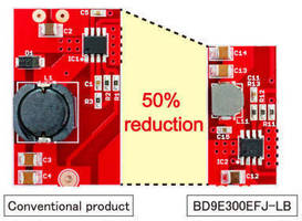
In addition, asynchronous rectification (diode rectification) system often used in high withstand voltage power application is not adopted but, instead, synchronous rectification system with built-in MOSFET is adopted for BD9E300EFJ-LB. Therefore, external transistor and rectification diode became unnecessary enabling 50% reduction of mounting area (Fig. 2).
Further, acceleration of switching action to 1 MHz enables use of compact inductor and capacitor. Its principle is shown below.
1) Downsizing of inductor
In order to downsize an inductor, it is usually necessary to reduce inductance, but that causes ripple of inductor current to become larger and necessity of large capacitor for output to occur (Fig. 3).
However, ripple current can be reduced without changing slope of triangular wave by raising switching frequency. For example, ripple current can be reduced to 1/2 by doubling frequency. Since inductance value is also reduced to 1/2 accordingly, downsizing of inductor can be realized (Fig. 4).
2) Downsizing of output capacitor
A switching regulator acts with rectangular wave between switch node and inductor. Inductor and output capacitor form secondary low-pass filter with which direct voltage is obtained by attenuating high frequency component of rectangular wave to smooth output voltage (Fig. 5).
Cutoff frequency fo of this low-pass filter usually fully attenuates switching frequency component fsw by setting the switching frequency at about 1/100. Since by raising switching frequency fsw cutoff frequency fo can also be raised, capacity value of output capacitor can be reduced and its downsizing becomes possible.
From this theory, whereas components are downsized by raising switching frequency, other problems become evident. They are switching loss of switch MOSFET and increase of gate charge loss that occur as switching frequency increases. Since they reduce efficiency and increase heat generation, they are minus factors for downsizing power source (Fig. 6).
Although there is a trade-off relation between switching frequency and switch MOSFET loss as shown above, the most advanced BiCDMOS process is adopted in BD9E300EFJ-LB to optimize balance between the two by designing with switching frequency of 1 MHz.
2.Reduction of loss by synchronous rectification system
The IC of asynchronous rectification system, which has been main stream of 24 V rail power supply system, uses MOSFET as the high-side switch and schottky diode as the low-side switch (Fig. 7).
When the high-side switch is turned on, input current is supplied from the high-side switch to load via inductor. At the same time, magnetic energy is accumulated in inductor and electric charge is accumulated in output capacitor. At the time, loss due to on resistance and current of MOSFET (Pd=R ON x I2) is generated.
In addition, when the high-side switch is off, the magnetic energy accumulated in inductor and the electric charge accumulated in output capacitor are discharged as current. The current returns to inductor via ground and schottky diode. At the time, loss due to forward-direction voltage and current of schottky diode (Pd=V F×I) is generated.
In the synchronous rectification system, on the other hand, loss is small because MOSFET with small on resistance is used also in low-side switch (Fig. 8).
For example, when 12 V is output from 24 V input, both the time while high-side switch is on and the time while low-side switch is on are 50%.
In the case of 5 V output from 24 V input, on the other hand, the time while high-side switch is on is 20.8% and the time while low-side switch is on is 79.2%, namely, loss of low-side switch is prevailing.
When current of 1 A is assumed to flow in low-side switch in the case of asynchronous rectification system, loss of the low-side switch will be Pd=V F×I=0.5V×1A=0.5W. On the other hand, in the case of synchronous rectification system, it is Pd=RON×I2=0.14Ω×1A2=0.14W so heat generation becomes 1/3.6 as much as that in the case of asynchronous rectification system.
Thus, in the case of large step-down ratio such as 5 V from 24 V rail power supply, synchronous rectification system is advantageous for downsizing because of smaller loss and lower heat generation.
3. Reduction of heat generation by process with large current and low loss
BD9E300EFJ-LB is produced by the most advanced BiCDMOS process of 0.35μm rule. Although the built-in switch part is composed of Nch-DMOS FET and usually there is a trade-off relation between high withstand voltage/low on resistance and low capacity gate, 40 V withstand voltage, 2.5 A current capacity, low on resistance of 170 mΩ and low gate capacity capable of 1 MHz action are realized. Because of this, heat generation is low even in the case of high frequency switching action.
In addition, since a package with its radiation pad exposed on its rear surface is adopted to enable efficient radiation even of the heat generated in IC chip, even a small package can be used at ease without fear of heat generation.
4. Power- and space-saving power supply IC series with 40 V withstand voltage
ROHM’s BD9E series is a new-generation solution that replaces asynchronous rectification (diode rectification) system which has long been mainly used in industrial equipment.
BD9E300EFJ-LB / BD9E301EFJ-LB and BD9E100FJ-LB / BD9E101FJ-LB are synchronous rectification step-down DC/DC converters of 1ch equipped with 40 V withstand voltage input. Efficiency of power transistor is enhanced by adoption of Nch-MOSFET at both high-side and low-side. In relation to the composition, a diode which is necessary for the bootstrap that forms gate drive of high-side Nch-MOSFET is also built-in.
Since the main difference among the four kinds is that output current of BD9E300 / BD9E301 is 2.5 A and that of BD9E100 / D9E101 is 1.0 A, MOSFET with lower on resistance and package with lower thermal resistance of which pad for radiation is exposed on its rear surface are adopted as a countermeasure against heat for BD9E300 / BD9E301 which handle larger power.
In addition, BD9E300 and BD9E100 are designed with switching frequency of 1 MHz. On the other hand, that for BD9E301 and BD9E101 is 570 kHz because when step-down ratio is high, switching loss increases resulting in toleration of no heat generation and inability of maintaining minimum on time with quick switching frequency. They are designed laying weight on efficiency rather than solution size (lower switching frequency decreases switching loss) and to enable customers to select switching frequency that matches their use condition.
5. Summary
Now that consciousness of energy saving is rising in every field, power devices and power supply ICs capable of dealing with large power utilizing semiconductors realizing energy saving are progressively adopted also in applications for industrial equipment dealing with large power. Further, when dealing with large power, withstand voltage that is higher than input voltage is required in order to prevent damage even when sudden surge voltage due to thunder, etc. is received.
ROHM is currently developing ICs with even higher withstand voltage to match such needs, and will continue to expand this DC/DC converter series prepare a wide variety of lineups to contribute to various markets.
Contacts
Elisabeth Sjo
AALTO INTERNATIONAL JAPAN Co. Ltd.
elisabeth@aaltoin.com
+81-50-5885-4936
Shinichi Tsusaka
AALTO INTERNATIONAL JAPAN Co. Ltd.
shin@aaltoin.com
+81-50-5885-4936
About ROHM Co., Ltd.
ROHM Semiconductor is a global company of 331,087 million yen (3,24billion $) revenue with 19.985 employees in the last fiscal year ending March 2014.