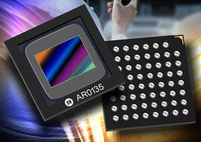
CMOS Image Sensor (1.2 MP) incorporates global shutter technology.
Press Release Summary:
Addressing needs of automotive imaging as well as high-speed barcode scanning and such emerging applications as VR and 3D depth sensing, AR0135 is capable of 54 fps at full resolution (1,280 x 960) and 60 fps at 720p. This 1/3 in. format, 1.2 MP imaging device, lets camera freeze fast moving scene data and ensures effective synchronization with pulsed light sources. Other features include dedicated FLASH and Trigger pins as well as parallel and serial (via 4-lane HiSPi interface) outputs.
Original Press Release:
ON Semiconductor Unveils Next Generation 1.2 Mpixel CMOS Image Sensor with Advanced Global Shutter Technology
New 1/3-Inch device delivers the functionality & robustness required for latest automotive, barcode scanning, and emerging virtual reality cameras
PHOENIX, Ariz. – ON Semiconductor (Nasdaq: ON), driving energy efficiency innovations, introduces another major advance in image sensing technology with the AR0135 global shutter CMOS image sensor. This 1/3-inch format, 1.2 MP imaging device has been designed to address the challenging requirements of automotive imaging as well as high-speed barcode scanning, and emerging applications like virtual reality and 3D depth sensing. The new global shutter sensor allows the camera to “freeze” fast moving scene data, and ensures effective synchronization with pulsed light sources.
The AR0135 sensor incorporates a new innovative global shutter pixel design, with 10X lower dark current and 4X higher shutter efficiency vs. previous generation products. These improvements allow the sensor to produce clear, low-noise images, in both low-light and bright scenes, and in high temperature environments. This performance enables the required eye tracking and gesture detection functionality in next generation automotive in-cabin systems, and improves the detection speed of barcode scanning systems.
This 1280 x 960 resolution device is capable of 54 frames per second (fps) at full resolution and 720p at 60 fps. AR0135 includes a broad set of features to improve overall system control, including dedicated FLASH and Trigger pins used to simplify control of external LED light sources, and more easily synchronize multiple sensors for stereo camera applications. The on-chip temperature sensor and statistics engine further enhance the diagnostic and control capability of the camera system. The AR0135 also provides the flexibility of both parallel and serial (via a four lane HiSPi interface) outputs.
“Global shutter technology is key to enabling challenging applications such as automotive driver monitoring and high-speed barcode scanning. These markets have a clear need for imaging solutions that combine high performance global shutter pixels with reliable operation in difficult environments,” states Ross Jatou, Vice President of the Automotive and Scanning Imaging Division at ON Semiconductor. “With the AR0135 we are well positioned to meet these demands. Our advanced global shutter pixel technology provides a new level of performance for next generation camera designs.”
Packaging and Availability
The AR0135AT is tested and qualified to meet the AEC-Q100 Grade 2 temperature range of -40 to 105°C, while the AR0135CS supports the standard temperature range of -30 to 70°C. Both are offered in a BGA-64 package or as a bare die. Engineering samples are available now, and the devices will be in production in 3Q16.
Follow @onsemi on Twitter: www.twitter.com/onsemi
About ON Semiconductor
ON Semiconductor (Nasdaq: ON) is driving energy efficient innovations, empowering customers to reduce global energy use. The company is a leading supplier of semiconductor-based solutions, offering a comprehensive portfolio of energy efficient power and signal management, logic, standard and custom devices. The company’s products help engineers solve their unique design challenges in automotive, communications, computing, consumer, industrial, medical and military/aerospace applications. ON Semiconductor operates a responsive, reliable, world-class supply chain and quality program, and a network of manufacturing facilities, sales offices and design centers in key markets throughout North America, Europe, and the Asia Pacific regions. For more information, visit http://www.onsemi.com.
ON Semiconductor and the ON Semiconductor logo are registered trademarks of Semiconductor Components Industries, LLC. All other brand and product names appearing in this document are registered trademarks or trademarks of their respective holders. Although the company references its Web site in this news release, such information on the Web site is not to be incorporated herein.
Contacts
Veronika Holscher
Media Relations
ON Semiconductor
(408) 660-2688
Veronika.Holscher@onsemi.com
Parag Agarwal Â
Vice President Investor Relations
ON Semiconductor
(602) 244-3437Â Â
Parag.Agarwal@onsemi.com