Wafer Inspection System handles advanced packaging applications. .
Press Release Summary:
Utilizing 3D laser triangulation technology, Wafer Scanner(TM) 3880 System provides 3D (height) and 2D measurement and inspection of micro and standard bumps, through silicon via post-via-fill copper protrusions, and re-distribution layers used in 3D IC packaging. High-resolution 3D sensor is designed specifically for micro bumps as small as few microns. Able to inspect flip chip and non-flip chip wafers, it also permits on-line or off-line defect review and classification.
Original Press Release:
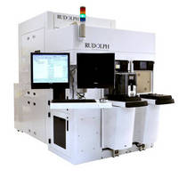
Rudolph Unveils New Wafer Scanner Inspection System
New WS 3880 system provides critical inspection and measurement capability for 3D advanced packaging applications
Flanders, New Jersey - Rudolph Technologies, Inc. (NASDAQ: RTEC), a leading provider of process characterization equipment and software for wafer fabs and advanced packaging facilities, announced today the availability of the new Wafer Scanner(TM) 3880 System, designed to be the fastest, most accurate and comprehensive inspection and measurement solution available for the rapidly developing technologies used in advanced packaging applications.
The WS 3880 provides 3D (height) and 2D measurement and inspection of micro and standard bumps, through silicon via (TSV) post-via-fill copper protrusions (nails) and re-distribution layers (RDL) used in 3D IC packaging. It also offers an ultra-high resolution 3D sensor designed specifically for micro bumps as small as a few microns. The WS 3880 is ideal for high-volume manufacturing, combining performance and throughput for either randomly sampled inspection or 100 percent inspection.
According to Reza Asgari, Rudolph's Wafer Scanner product manager, "Micro bumps, TSVs and RDLs are critical interconnect technologies used in 3D IC packages; the new WS 3880 provides the 2D and 3D measurement and inspection capability required to develop and maximize yields for these packaging processes. Ultra-high resolution allows the Wafer Scanner to accurately characterize small features, such as micro bumps and TSV nails, which manufacturers are using to achieve unprecedented connection densities between chips, while still preserving the flexibility to handle standard bumps and other larger features."
Asgari added, "Flexibility, throughput and inspection performance were primary considerations for the first production system, delivered in March 2011 to a major semiconductor foundry. The ability to look at a range of bump and RDL sizes and types was critical for the second system that shipped to a leading IDM where it will be used to develop new packaging processes."
The WS 3880 replaces the highly successful 3840 system, launched immediately following Rudolph's acquisition of RVSI assets in 2008. Over 20 WS 3840 systems have been installed in advanced packaging facilities.
The WS 3880 is a comprehensive wafer inspection system, providing a fast, flexible and reliable inspection and metrology solution for bump, RDL and TSV nail processes in advanced semiconductor device packaging. It can inspect both flip chip and non-flip chip wafers. The base system provides high throughput, image-based macro defect inspection, as well as measurements of bump diameter and position, RDL width, and other 2D parameters. Rudolph's proprietary 3D laser triangulation technology measures bump height and coplanarity, RDL thickness, and much more. The system permits on-line or off-line defect review and classification. Electronic wafer maps can be imported into the system, updated after inspection and exported.
The WS 3880 system is now commercially available and can be ordered immediately. For more information, please visit www.rudolphtech.com or email info@rudolphtech.com.
Rudolph Technologies, Inc. is a worldwide leader in the design, development, manufacture and support of defect inspection, process control metrology, and data analysis systems and software used by semiconductor device manufacturers worldwide. Rudolph provides a full-fab solution through its families of proprietary products that provide critical yield-enhancing information, enabling microelectronic device manufacturers to drive down the costs and time to market of their products. The company's yield management solutions are used in both the wafer processing and final manufacturing of ICs, as well as in emerging markets such as LED and Solar. Headquartered in Flanders, New Jersey, Rudolph supports its customers with a worldwide sales and service organization. Additional information can be found on the company's web site at www.rudolphtech.com.