Wafer Handler improves microelectronics industry yield.
Press Release Summary:
In addition to offering 360° rotation for full macro examination of wafer's back surface and edges, AL120(TM) can transfer 100-200 mm dia wafers with thicknesses down to 90 µm to meet demands of thin-wafer manufacturing. Recipe-driven tool can be programmed for different configurations, while pushbutton recipe selection allows operator to load different products instantly. System can also be adapted for smaller-diameter wafers and used with non-Olympus microscope models on custom basis.
Original Press Release:
Olympus AL120(TM) Wafer Handler Designed for Wafers Down to 90µm in Thickness, Improving Yield and Productivity for the Microelectronics Industry
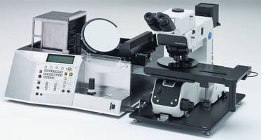
The Olympus AL120(TM) wafer handling system is the newest generation of the company's AL wafer handling systems, delivering the renowned performance and reliability for which Olympus microelectronics products are known. The AL120 wafer handler transfers wafers with thicknesses down to 90µm to meet the demands of thin-wafer manufacturing. The new system offers 360-degree rotation, for full macro examination of the wafer's back surface and edges.
The tool is user friendly and recipe driven; it can be programmed for different configurations, including specific cassette types, wafer specifications and transfer speeds. Quick push-button recipe selection allows the operator to load different products instantly. The AL120 also can be adapted for smaller-diameter wafers and used with non-Olympus microscope models on a custom basis.
The AL120 wafer handler accepts wafers that are 100-200mm in diameter. It can be fully integrated with the full line of Olympus MX dedicated wafer inspection microscopes, which provide exceptional image resolution and clarity through a wide range of observation methods. The combination of the AL120 with the MX series microscopes provides a complete inspection system, which also can be configured with the MX -IRP Inspection and Review software for a fully automated inspection station solution.
Olympus continues to focus attention on both wafer and operator safety by adhering to SEMI S2 and S8 standards for semiconductor handling and inspection equipment. In line with the Olympus corporate focus on environmental protection, the AL120 wafer handler is fully compliant with international Reduction of Hazardous Substances (RoHs) standards.
With its flexible design and robust performance, the AL120 will meet and exceed the needs of semiconductor manufacturers for reducing wafer contamination, increasing throughput and improving overall yield.
For more information on the Olympus AL120 wafer handler, contact Jennifer Wrigley at Olympus America Inc., 3500 Corporate Parkway, Center Valley, PA 18034-0610 USA; phone (484) 896-5213, e-mail Jennifer.Wrigley@olympus.com, or visit http://www.olympusamerica.com/AL120.