TEM Sample Preparation Workflow promotes high throughput.
Press Release Summary:
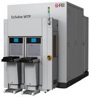
Suitable for use in transmission electron microscopy (TEM) analysis, ExSolve™ can prepare site-specific, 20 nm thick TEM lamella on whole wafers up to 300 mm dia. Solution can sample many sites per wafer in fully automated process inside fab, and wafer TEM prep (WTP) increases speed of sample preparation. This provides semiconductor and data storage manufacturers with access to data needed to verify and monitor process performance. FOUP handling capability is standard.
Original Press Release:
FEI Announces New ExSolve High-Throughput TEM Sample Preparation Workflow
ExSolve enables semiconductor and data storage manufacturers to obtain more information faster and at lower cost for process verification.
Hillsboro, Ore. — FEI (NASDAQ: FEIC) today released ExSolve™, an automated, high-throughput sample preparation workflow for transmission electron microscopy (TEM) analysis. The ExSolve wafer TEM prep (WTP) dramatically reduces the cost and increases the speed of sample preparation, providing semiconductor and data storage manufacturers with quick and easy access to the data they need to verify and monitor process performance. ExSolve can prepare site-specific TEM lamella, sampling many sites per wafer in a fully-automated process inside the fab, giving semiconductor manufacturers much more information than conventional approaches, while at the same time reducing the capital cost of sample preparation by up to 70 percent.
“TEM analysis is the only method that allows semiconductor manufacturers to fully characterize, understand and control their advanced manufacturing processes, such as three-dimensional and multi-gate devices, at the 20nm node and smaller. Until now, most sample preparation for TEM analysis has used slow, manual processes that break the wafer into multiple hard-to-track and hard-to-handle pieces,” states Rudy Kellner, vice president and general manager of the Industry Group at FEI. “ExSolve fully automates lamella creation from whole wafers, eliminating most of the manual sample handling and data tracking overhead. We expect ExSolve to transform the way process engineers think about process data. Instead of trying to make the most of a minimal sampling plan, they can now have fast, inexpensive access to all the data they need for thorough process verification.”
The ExSolve WTP system is an automated, high-throughput sample preparation system that can prepare site-specific, 20nm thick lamellae on whole wafers up to 300mm in diameter. It is part of a fast, complete workflow that includes TEMLink™, and the Metrios™ TEM. The ExSolve includes FOUP handling and is designed to be located in the fab near the manufacturing line.
The ExSolve WTP workflow addresses the needs of customers that require automated, high-throughput sampling at advanced technology nodes. It complements the capabilities of FEI’s Helios NanoLab™ DualBeam™ 1200AT, which provides more flexible, operator-directed, sample preparation methods, along with additional capabilities such as high-resolution scanning electron microscopy (SEM) imaging and analysis.
For more information about the ExSolve WTP workflow, please visit www.FEI.com/ExSolve.
About FEI
FEI Company (Nasdaq: FEIC) designs, manufactures and supports a broad range of high-performance microscopy workflow solutions that provide images and answers at the micro-, nano- and picometer scales. Its innovation and leadership enable customers in industry and science to increase productivity and make breakthrough discoveries. Headquartered in Hillsboro, Ore., USA, FEI has over 2,500 employees and sales and service operations in more than 50 countries around the world. More information can be found at: www.fei.com.