Solder Paste Inspection System features 5D technology.
Share:
Press Release Summary:
Featuring patented sensor technology that can simultaneously combine 2D and 3D image processing, Model S1 mkll minimizes inspection tolerances over entire PCB, enabling users to watch for process drift. System performs true area, shape, volume, offset, and height measurements, providing yield optimizing process control, while tuning and monitoring printer settings before problem spreads throughout entire production run.
Original Press Release:
MEK's Latest 5D SPI System Features Patented New Sensor Technology
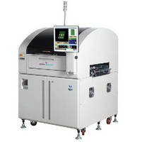
Mek Europe BV, formerly known as Marantz Business Electronics, recently launched their latest automated Solder Paste Inspection system. The Model S1 mkII features patented second generation sensor technology that enables unique, simultaneous 2D and 3D inspection.
The resultant high speed 5D technology measures beyond the bounds of apertures with 2D/3D comparative analysis that can determine slump and release defects. The newly re-engineered inspection head has improved 2D image capture providing enhanced accuracy and repeatability surpassing all existing systems, especially important for the thinner stencils and smaller component pads of tomorrow.
The S1 mkII is capable of defect detection beyond anything previously possible, because it incorporates patented sensor technology that can simultaneously combine 2D and 3D image processing. The new technology allows a vast reduction of wide inspection tolerances, typical of most SPI systems. True area, shape, volume, offset and height measurements are provided in combination, providing genuine yield enhancing process control and a perfect tool to tune and monitor printer settings before a problem spreads throughout an entire production run.Â
Jeremy Saise, Mek Technical Director further explained, “This is a revolutionary, process control tool that enables users to quickly and easily tune and adjust their print process. We have introduced Production Control Mode. You see, most SPI are utilized only to improve process control, and are left with wide tolerances to accommodate varied paste releases. The Mek S1 can automatically understand these varied releases and bring the real world of printing in to its tolerances. Tighter tolerances over the whole PCB, enabling the user to watch for process drift which was previously difficult or impossible to capture. Only the S1 can do this.”
SPI equipment is essential to monitor and control the most critical, error prone process step in manufacturing defect free electronic assemblies, solder paste printing. The interception of print defects reduces rework costs, delivers instant yield improvement and accelerates ROI
About MEK Europe BV
A former division of Marantz well known for its high quality Audio/Video products, MEK Japan (Marantz Electronics Kabushiki Kaisha), developed its first AOI system in 1994. Developed to inspect PCB assemblies for correct component placement and soldering, the company’s original AOI system was designed for use in Marantz factories. Proving to be a highly successful, cost-effective alternative to traditional human inspection, MEK developed its first generation commercial system in 1996. With a steadily growing installed base, MEK Japan and its European headquarters, MEK Europe BV, have sold over 5000 units worldwide to date. Now well established as a leading force in AOI technologies, the company recently launched a 5D post-print SPI system which combines 3D and 2D image processing methodologies to deliver unprecedented defect detection.
MEK Europe BV Contact
Henk Biemans
MEK Europe
PO Box 12
5688 ZG
Oirschot
The Netherlands
Tel: +31 40 71 14 111
Email: info@mek-europe.com
www.mek-europe.com Â