Photo-Etched Lead Frames target IC manufacturers.
Press Release Summary:
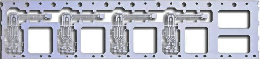
Ranging in thickness from 0.5–40 mil with features as small as 4 mil on 0.010 in. centers, Photochemically-Etched Surface-Mount and Insert-Mount Lead Frames are suitable for semiconductors, glass-to-metal seals, and relays as well as medical applications. Single-or double-sided frames can be plated in their entirety or selectively using base materials such as kovar, nickel-iron alloys, copper alloys, and pure nickel. Lead-free plating materials include silver, nickel, gold, or tin.
Original Press Release:
Custom-Designed Photo-Etched Lead Frames from PEI Meet Exacting Electrical, Thermal Conductivity and Strength Requirements of IC Manufacturers
Milford, MAÂ -- Photofabrication Engineering (PEI) has expanded its manufacturing capabilities for custom-designed, photochemically-etched surface-mount and insert-mount lead frames for integrated circuit manufacturing. These lead frames are used in a wide variety of applications including semiconductors, glass-to-metal seals, and relays, as well as medical applications such as hearing aids.
Using base materials such as kovar, nickel-iron alloys, copper alloys, and pure nickel, PEI can plate lead frames in their entirety or selectively. Lead-free plating materials include silver, nickel, gold, or tin, depending on the customer’s specific electrical and thermal conductivity requirements. Since the lead frame is the main conduit by which heat flows from the chip to the printed circuit board, PEI selects the manufacturing material to maximize the device’s operating life for any given application or environment.
PEI manufactures high-density lead frames with acute profiles and ultra-fine pitches, allowing for high pin counts. Single- or double-sided lead frames are etched without incurring the stresses associated with typical machining methods. More importantly, PEI’s process can be used for lead frames that are too complicated for stamping. Dimensions can be held to extremely tight tolerances, with no burrs or other surface irregularities.
PEI’s lead frames range in thickness from 0.5 mil [0.0127 mm] to 40 mil [1.575 mm], with features as small as 4 mil [0.10 mm] on 0.010 in. [0.254 mm] centers, creating lead frames that are strong enough to be handled yet flexible enough to allow bending when necessary.
A significant advantage of photochemical etching is the ability to reproduce large quantities of parts without tooling “wear”--the millionth part is exactly the same as the first part. Changes to tools can be implemented quickly, and phototools are significantly less expensive than traditional tools—ideal for manufacturing plates from prototype to production quantities with short turnaround times (about 10% of those for stamped frames).
Established in 1968, PEI has approximately 50 employees and is ISO 9001:2008; AS9100 and ITAR certified. To understand more about the photo chemical etching process visit http://www.photofabrication.com/etching-process/ or view the short PEI YouTube video.
For more information about PEI’s lead frames and other photoetched products, contact Chip Lehrer, President, Photofabrication Engineering, Inc., 500 Fortune Boulevard, Milford, MA 01757; telephone +(508) 478-2025; FAX+(508) 478-3582; e-mail sales@photofabrication.com; or visit http://www.photofabrication.com.
Judy Grande, Marketing Manager
978-807-5831 cell
508-478-2025 x120
jgrande@photofabrication.com
www.photofabrication.com
www.decorativeetching.com
PEI (Photofabrication Engineering Inc.)
500 Fortune Boulevard, Milford, MA 01757