Panel Lithography System supports advanced packaging.
Press Release Summary:
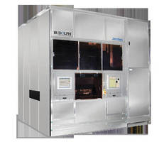
Capable of processing both glass and organic laminate panels in semiconductor advanced packaging market, JetStep™ features on-the-fly autofocus for thick photoresists, onboard reticle library, and 6 second reticle change out wheel. System can utilize company's suite of software products, including ProcessWORKS® for run-to-run control, Discover® for yield management, and ARTIST® for fault detection and classification.
Original Press Release:
Rudolph Announces the JetStep Panel Lithography System for Advanced Packaging
Unique stepper design is driven by the semiconductor advanced packaging transition from wafer to panel manufacturing
Flanders, New Jersey —Rudolph Technologies, Inc. (NASDAQ: RTEC), a leading provider of process characterization, photolithography equipment and software for the semiconductor, FPD, LED and solar industries, today announced the Company’s entry into the emerging advanced packaging panel lithography market with the innovative JetStep™ Panel Lithography System, the latest technological evolution in Rudolph’s total lithography solution.
COO Benefits Drive Revolutionary Change in Advanced Packaging Photolithography
Scalable technology is rapidly increasing in importance. To improve their cost of ownership (COO) and increase productivity, advanced packaging facilities are transitioning to large panels ranging up to Gen 3.5 (approximately 650mm x 720mm). Enlarging the substrate size has been the natural approach, however, traditional technology has been limited to standard wafer sizes. With companies progressively moving to fan-out packages, they are no longer limited to operating within the constraints of a round wafer.Â
By responding to market opportunities and addressing the stringent demands of their customers’ technical roadmaps, Rudolph is optimally positioned to capture first mover advantage in the emerging market of advanced packaging panel lithography. Customers could require wafer tool suppliers to redesign their tools to handle large panels, or they could have panel tool suppliers learn how to expose semiconductors. Rudolph’s unique tool design provides a compelling solution by delivering against both sets of requirements, while avoiding the risks inherent in any development program undertaken by a panel or wafer tool supplier. The JetStep Panel Lithography System, having emerged from the flat panel display market, is readily capable of processing both glass and organic laminate panels in the semiconductor advanced packaging market.
“Moving from reconstituted wafers to chips-on-panels is a significant, natural evolution of the advanced packaging platform,” said Elvino da Silveira, chief technology officer of Rudolph’s Lithography Systems Group. “This new substrate size is uniquely suited to Rudolph’s expertise in advanced packaging applications as well as panel-processing capabilities. The stepper’s inherent ability to handle panels reinforces the strategic vision behind this product introduction and market entry.”
As resolution, overlay and other technical specifications become more critical in advanced packaging processes, back-end manufacturers are choosing to move from aligners to steppers to meet these requirements. The JetStep Panel Lithography System, combining unique LCD manufacturing and advanced packaging features and requirements, joins the previously announced JetStep Lithography System for general advanced packaging lithography. In addition to on-the-fly autofocus for thick photoresists, an onboard reticle library and six-second reticle change out wheel, the JetStep Panel Lithography System can utilize Rudolph’s suite of software products— ProcessWORKS® Software for run-to-run control, Discover® Software for yield management and ARTIST® Software for fault detection and classification—to provide a comprehensive solution for virtually any advanced packaging application.
“Rudolph has the technological foundation required for a panel lithography system,” noted Paul F. McLaughlin, chairman and chief executive officer. “Our combined application knowledge in advanced packaging and flat panel display ideally positions us to lead the way in this new market. Our vision for Rudolph is to establish the Company as the vendor of choice for advanced packaging and photolithography solutions. We have been working in close collaboration with our customers to further define solutions in accordance with their roadmaps. The biggest advantage provided to our customers is in throughput, as the number of die that can be processed in a given amount of time results in a compelling COO advantage over wafers. The introduction of the JetStep Panel Lithography System further solidifies our market-leading position. While we anticipate adoption of the new system in mid-2014, we are currently demonstrating this panel exposure technology today in our lithography manufacturing facility in Wilmington, Massachusetts.”
For more information about Rudolph’s JetStep Panel Lithography System, visit www.rudolphtech.com.
About Rudolph Technologies
Rudolph Technologies, Inc. is a worldwide leader in the design, development, manufacture and support of defect inspection, advanced packaging lithography, process control metrology, and data analysis systems and software used by semiconductor device manufacturers worldwide. Rudolph provides a full-fab solution through its families of proprietary products that provide critical yield-enhancing information, enabling microelectronic device manufacturers to drive down the costs and time to market of their products. The Company’s expanding portfolio of equipment and software solutions is used in both the wafer processing and final manufacturing of ICs, and in adjacent markets such as FPD, LED and Solar. Headquartered in Flanders, New Jersey, Rudolph supports its customers with a worldwide sales and service organization. Additional information can be found on the Company’s website at www.rudolphtech.com.
Contacts:
Trade Press:
Amy Pauling
952.259.1794
amy.pauling@rudolphtech.com