PCB Electrical Test System handles 3D packages.
Press Release Summary:
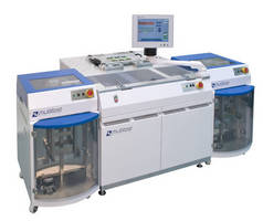
Multitest Plug & Yield system, for in-process test in 3D assembly, consists of InStrip3D PCB handling machine and test interface board. Product requires minimum contact force, with inclusion of vertical spring contacting solution, to avoid stress on sensitive bare dies. Supporting fine-pitch, high layer count PCBs, system can support 0.4 mm pitch array application in high pin count multi-site configuration.
Original Press Release:
Multitest's Solution for 3D Packages Released to Production
Electrical test during the assembly process ensures best production yield
Rosenheim, Germany - Multitest, a designer and manufacturer of final test handlers, contactors and load boards used by integrated device manufacturers (IDMs) and final test subcontractors worldwide, announces that the first Multitest Plug & Yield solution for the test of 3D packages recently has been released to the customer's production.
James Quinn, VP Sales and Marketing, commented: "Multitest is the first equipment supplier to deliver a full turnkey hardware setup for in-process test in 3D assembly. Our unique product portfolio enables us to partner with our customers to develop comprehensive solutions for this emerging packaging technology that we see as a major strategic initiative in the semiconductor industry."
The fully integrated setup consists of a Multitest InStrip3D, a test interface board and a contacting solution based on vertical spring technology. The system will be used for electrical test partial stacks during assembly of a mobile SoC.
The InStrip3D utilizes the experience gained from a well-established installed base of high-parallel InStrip/InMEMS solutions. The architecture of the InStrip allows the configuration of the system to meet the special requirements of partial stack test with respect to the extremely sensitive bare dies.
Multitest's contactor division developed a solution that ensures reliable contacting yield, but only requires a minimum contact force in order to avoid stress on the extremely sensitive bare dies.
The integrated test solution uses a Multitest load board, leveraging the industry-leading fabrication capabilities for fine-pitch, high layer count PCBs to support this 0.4 mm pitch array application in a high pin count multi-site configuration. In close cooperation with the customer, the mechanics of the test were redesigned to accommodate the increased forces from the highly dense pogo array of approximately 6000 pins.
Combining the engineering expertise and capabilities of all three product groups, Multitest developed a fully integrated solution that optimally solves the challenges of a highly sensitive device in a cost efficient multi-site setup. The final Plug & Yield solution enables highly-parallel electrical in-process test of stacked dies during the assembly process of 3-D packages.
With the growing importance of 3-D integration, Multitest sees a great need for cost-efficient in-process test during the package assembly. The current concept of KGD and final test before shipment does not cover the risk during the assembly of multiple dies.
James Quinn asserts: "Initially 3D packaging created challenges in wafer level processes, such as deep silicon etch and wafer processing. With these challenges being addressed, the industry now faces the need to develop advanced test strategies. Insufficient test strategies will be a hurdle for a broader acceptance of 3D integration, particularly when it comes to TSV. At the same time we are convinced that smart approaches for optimal test insertion points will make test a key differentiator."
Multitest will display the InStrip3D at its Open House in Santa Clara from July 10-12, 2012 (www.multitest.com/openhouse). High parallel test of 3D packages also will be part of the presentation given by Bernhard Lorenz, Vice President Engineering, at the Test Vision 2020 Conference held in conjunction with SEMICON West (www.multitest.com/SemiconWest). For more information, visit http://www.multitest.com/3DIntegration.
About Multitest
Multitest (headquartered in Rosenheim, Germany) is one of the world's leading manufacturers of test equipment for semiconductors. Multitest markets test handlers, contactors and ATE printed circuit boards. Multitest has more than 30 years of experience in the semiconductor industry, providing solutions to the automotive, consumer and communication but also to the sensor market. Globally, more than 900 employees serve the company's customers in offices and branches in North America, Singapore, Malaysia, the Philippines, Taiwan, China and Thailand.
www.multitest.com