P-Channel Gen III Power MOSFET measures 2.4 x 2.0 x 0.4 mm.
Press Release Summary:
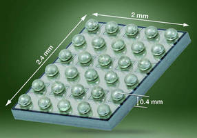
Supplied in 30-pin CSP MICRO FOOT® package with 0.4 mm profile, Si8851EDB increases efficiency while conserving space in mobile computing devices. This -20 V TrenchFET® p-channel Gen III power MOSFET offers on-resistance of 8.0 and 11.0 mΩ at respective gate drive of -4.5 and -2.5 V. Optimized for load and battery switches in power management applications for tablets, smartphones, and notebooks, halogen-free and RoHS-compliant device also provides 6 kV typ ESD protection.
Original Press Release:
Vishay Intertechnology's -20 V P-Channel Gen III MOSFET Is First in 2.4 mm by 2.0 mm by 0.4 mm MICRO FOOT® Package Size
For Mobile Computing Devices, Space-Saving MOSFET Offers Low On-Resistance Down to 8.0 mΩ at -4.5 V
MALVERN, Pa. — Vishay Intertechnology, Inc. (NYSE: VSH) today extended its offering of TrenchFET® p-channel Gen III power MOSFETs with the industry's first -20 V device in the 2.4 mm by 2.0 mm by 0.4 mm CSP MICRO FOOT® package size. Designed to increase efficiency and save space in mobile computing devices, the Vishay Siliconix Si8851EDB offers extremely low on-resistance of 8.0 mΩ and 11.0 mΩ at -4.5 V and -2.5 V gate drives, respectively.
The Si8851EDB's p-channel Gen III technology, in combination with MICRO FOOT's packageless CSP technology and 30-pin design and layout, provides the lowest on-resistance possible for a given outline area. Compared with the closest competing 2 mm by 2 mm by 0.8 mm device, the Si8851EDB combines a 50 % thinner profile with almost half the on-resistance at a 4.5 V gate drive, providing 37 % lower on-resistance per package size. Offering similar on-resistance to 3.3 mm by 3.3 mm by 0.8 mm MOSFETs, the Si8851EDB provides a 56 % smaller outline and at least a 30 % lower on-resistance per package size.
With its slim 0.4 mm profile, the device released today is optimized for load and battery switches in power management applications for tablets, smartphones, and notebooks. The Si8851EDB's low on-resistance allows designers to achieve lower voltage drops in their circuits — promoting more efficient use of power and longer battery run times — while its compact footprint saves valuable PCB space. High typical ESD protection to 6 kV helps protect handheld devices against static charges while ensuring safe part handling during the manufacturing process. The MOSFET is halogen-free according to the JEDEC JS709A definition and compliant to RoHS Directive 2011/65/EU.
The Si8851EDB is the latest expansion to Vishay's MICRO FOOT family, which can be found at http://www.vishay.com/mosfets/micro-foot-package/. More information on the company's lineup of p-channel Gen III MOSFETs is available at http://www.vishay.com/mosfets/geniii-p/.
Samples and production quantities of the Si8851EDB are available now, with lead times of 12 to 16 weeks for larger orders. Pricing for U.S. delivery only starts at $0.15 per piece in 100,000-piece quantities.
Vishay Intertechnology, Inc., a Fortune 1000 Company listed on the NYSE (VSH), is one of the world's largest manufacturers of discrete semiconductors (diodes, MOSFETs, and infrared optoelectronics) and passive electronic components (resistors, inductors, and capacitors). These components are used in virtually all types of electronic devices and equipment, in the industrial, computing, automotive, consumer, telecommunications, military, aerospace, power supplies, and medical markets. Vishay's product innovations, successful acquisition strategy, and "one-stop shop" service have made it a global industry leader. Vishay can be found on the Internet at www.vishay.com.
TrenchFET and MICRO FOOT are registered trademarks of Siliconix incorporated.
http://twitter.com/vishayindust
http://www.facebook.com/VishayIntertechnology