FIB SEM System investigates materials at nanometer scale.
Press Release Summary:
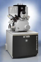
Combining high-resolution scanning electron microscope with focused ion beam milling, Helios NanoLab™ 660 DualBeam™ is used to investigate structure and function of materials at nanometer scale, create prototypes of micro and nano electro-mechanical systems, and prepare ultrathin samples for atomic scale imaging and analysis in TEM. NanoBuilder™ 2.0 nanoprototyping toolset automatically fabricates 3D prototypes of nano- and microscale devices from computer-generated models.
Original Press Release:
FEI's New Helios NanoLab 660 DualBeam Sets New Standard for Imaging and Milling Performance
Latest generation of FEI’s industry-leading DualBeam for materials science research to be showcased at the 7th International Conference on Materials for Advanced Technologies, 30 June to 5 July, 2013, Suntec, Singapore.
FEI will showcase its new Helios NanoLab™ 660 DualBeam™, at the upcoming Materials Research Society conference in Singapore. The Helios NanoLab 660 DualBeam system provides one of the highest imaging resolution and contrast SEMs, combined with one of the fastest and most precise FIB milling performances of any commercially-available focused ion beam/scanning electron microscope (FIB/SEM) system.    Â
DualBeam (FIB/SEM) systems are used to investigate the structure and function of materials at the nanometer scale, create prototypes of micro and nano electro-mechanical systems (MEMS and NEMS), and prepare ultrathin samples for atomic scale imaging and analysis in a transmission electron microscope (TEM).
“The Helios NanoLab 660 DualBeam adds our second-generation extreme high-resolution (XHR) SEM capability to the proven Helios DualBeam platform to provide sub-nanometer imaging resolution over a wide range of accelerating voltages. Its precise selective contrast enhancement can be tailored to reveal the finest details of the sample’s topography, structure, composition and more,” said Trisha Rice, vice president and general manager, Materials Science Business Unit, FEI. “The combination of high-resolution, high-contrast imaging and high-performance milling allows researchers to access more accurate information from their sample in less time. A new high-current mode enables faster analysis.”
“The Helios NanoLab DualBeam is indispensable for high-resolution imaging of surfaces, sections or volumes of a wide variety of materials, especially soft or delicate samples, such as carbon nanotubes, polymers, ceramics, catalysts, etc.,” added Rice. “The SEM’s exceptional performance at low accelerating voltages, reduces beam damage, and dramatically improves sensitivity to surface detail.”
NanoBuilder™ 2.0, a second-generation nanoprototyping toolset now introduced on the Helios NanoLab 660, automatically fabricates 3D prototypes of nano- and microscale devices, such as nanosensors from computer-generated models, and thereby simplifies and accelerates the prototyping workflow. Starting with a CAD design, the NanoBuilder software directs FIB milling and deposition to build intricate 3D structures with features ranging in size from nanometers to millimeters.
FEI’s second-generation XHR SEM uses proprietary electron optical and detector technologies to deliver sub-nanometer imaging resolution, with high signal collection efficiency and high contrast, over the widest range of accelerating voltages (0.5-30 kV). Fast time to data is enabled both by the new in-column detection, which allows simultaneous topographic and materials contrast imaging and precise materials information from triple backscattered electron filtering, and by the new high-current SEM mode, which delivers up to 100 nA in a micrometric spot. The Tomahawk™ FIB column guarantees the tightest beam at high and low currents, for fast, precise large-volume removal and polishing, respectively; and exceptional low-energy performance, to remove surface damage in the final polishing steps of thin sample preparation.
To optimally serve nanoprototyping and sample preparation applications, the Helios NanoLab 660 DualBeam continues to support FEI’s latest technology advancements, such as the EasyLift™ nanomanipulator, for the fastest, most reliable thin sample preparation using the in situ lift out (INLO) method, and the MultiChem™ gas injector system, for gas-assisted etching and beam-induced deposition of materials with higher speed and quality, added flexibility and optimal process control.
For more information, please visit FEI at the 7th International Conference on Materials for Advanced Technologies, 30 June to 5 July, 2013, Suntec, Singapore.
About FEI
FEI (Nasdaq: FEIC) is a leading supplier of scientific instruments for nano-scale applications and solutions for industry and science. With more than 60 years of technological innovation and leadership, FEI has set the performance standard in transmission electron microscopes (TEM), scanning electron microscopes (SEM) and DualBeams™, which combine a SEM with a focused ion beam (FIB). FEI has over 2,500 employees and sales and service operations in more than 50 countries around the world. More information can be found at: www.fei.com.