Dielectric Deposition System is designed for 3D chip packaging.
Press Release Summary:
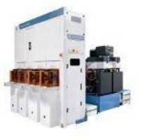
Applied Producer® InVia(TM) dielectric deposition system uses CVD process to deposit uniform, thick oxide films in greater than 10:1 high aspect ratio (HAR) through-silicon via (TSV) structures. Process also enables electrical isolation of TSV to ensure reliable performance. For 3D packaging schemes, it electrically connects chips that are vertically stacked to boost speed and lower power consumption.
Original Press Release:
Applied Materials Introduces Critical Via Liner Technology for 3D Chip Packaging
SANTA CLARA, Calif. - Applied Materials, Inc. today added to its extensive line of 3D chip packaging solutions with the launch of its Applied Producer® InVia(TM) dielectric deposition system. Using a unique CVD* process, the InVia system delivers an innovative method for depositing the critical oxide liner film layer in high aspect ratio (HAR) through-silicon via (TSV) structures. Providing conformal coverage over the full depth of these challenging features, the InVia process enables robust electrical isolation of the TSV - which is vital for reliable device performance.
"With the launch of the InVia system, we now provide customers with a comprehensive solution for fabricating high aspect ratio TSVs"
TSVs play a key role in emerging 3D packaging schemes, electrically connecting chips that are vertically stacked to boost speed and lower power consumption. Two primary techniques, called via-first and via-middle, in which the TSVs are fabricated along with the device's transistor and interconnect layers, offer superior design flexibility and device functionality, but have presented a significant challenge for insulating liner processes. The InVia system's proprietary process technology meets the challenges of both techniques, depositing uniform, thick oxide films in greater than 10:1 HAR vias while meeting thermal budget requirements.
Implemented on Applied's award-winning Producer GT(TM) platform, the InVia system offers compelling advantages over competing technologies. The system has much higher throughput than batch furnaces, with the capability to process up to eight times more wafers per hour at less than half the cost, especially when depositing very thick liners for high performance applications. Competing PECVD* systems are unable to deposit oxide films evenly in deep, narrow vias, making this approach unsuitable for HAR applications.
"With the launch of the InVia system, we now provide customers with a comprehensive solution for fabricating high aspect ratio TSVs," said Bill McClintock, vice president and general manager of Applied's DSM* and CMP* business unit. "From etch and via liners, to metal fill and planarization, we can offer chip manufacturers a cost-effective, rapid path to implement their most challenging 3D packaging schemes and quickly bring their exciting new products to market."
For more information on Applied's broad range of systems for 3D chip packaging applications, visit appliedmaterials.com/3d_integration.
Applied Materials, Inc. (Nasdaq:AMAT) is the global leader in Nanomanufacturing Technology(TM) solutions with a broad portfolio of innovative equipment, service and software products for the fabrication of semiconductor chips, flat panel displays, solar photovoltaic cells, flexible electronics and energy efficient glass. At Applied Materials, we apply Nanomanufacturing Technology to improve the way people live. Learn more at www.appliedmaterials.com.
* CVD: chemical vapor deposition, PECVD: plasma-enhanced CVD, DSM: dielectric systems and modules, CMP: chemical-mechanical planarization