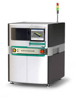
Automated Optical Inspection System has 3D capability.
Share:
Press Release Summary:
Combining 3D measurement with 2D AOI technology, Zenith system detects all kinds of solder joint defects on whole assembled PCB surfaces based on their true profilometry, as well as simple defects such as tombstoning, while measuring dark components, lifted leads, or mislocated devices. System can be programmed within 30 min, as it automatically extracts all necessary information about components to be inspected by APLB (Automatic Package Library Builder).
Original Press Release:
Koh Young "Breaks the 2D AOI Barrier" with Revolutionary New 3D AOI Technology
April 20, 2009
Seoul, Korea - Koh Young Technology, a recognized global leader in advanced Solder Paste Inspection (SPI) technology, announces the launch of a new family of Automated Optical Inspection (AOI) systems, the Koh Young Zenith series.
This new family of systems incorporates revolutionary new 3D inspection technology. The new Zenith system is based on technology which 'breaks the 2D AOI inspection barrier' by incorporating the ability to sense and measure the Z-axis profilometry of whole assembled PCB surfaces, including electronic components, solder joints, patterns, holes, and even components with foreign material on them. The Zenith's 3D capability operates in addition to full conventional 2D AOI; thus, Zenith eliminates the traditional shortcomings of 2D AOI which make it vulnerable to in escapes, false calls and inspection errors.
After many years of research and solving multiple 3D imaging problems, Koh Young introduced this new technology at the recent IPC/APEX 2009 show. The new technology is being introduced to the global market over the next few weeks at exhibitions in Asia and Europe.
In making the announcement, Dr. Kwangill Koh, President and CEO, said "2D imaging is the commonly-used technology in AOI inspection systems, but it has a number of shortcomings that are well known to users, such as false calls, escapes and long programming times. Until now, a better technology has not been available. But that is all changed now with the introduction of the Zenith system."
Dr. Koh adds that "The challenges facing 3D AOI were complex, but we solved all common bottlenecks of 3D measurement such as specular problems associated with shiny solder joints, and projection obstacle problems due to relatively higher electronic components. We have also solved object and reference plane shadow problems between the adjacent leads of fine pitch QFPs with our proprietary eight-way projection system. We are providing a much greater measurement range while maintaining the high resolution known from our Paste Measurement Systems, expanding on our patented 3D technology."
The new Zenith system uniquely combines 3D measurement with 2D AOI technology. The ability to measure the height and shape of components and shiny solder joints allows a true comparison with the IPC 610 Acceptability Standard. Thus, there is no question regarding the acceptability of the solder joint.
With its 3D technology, Zenith easily detects not only all kinds of solder joint defects based on their true profilometry, but also simple defects such as tombstoning and has no problems measuring dark components, lifted leads or mislocated devices without any confusion as in conventional 2D AOI systems. Programming is simple enough to require less than 30 minutes, because the new Zenith system automatically extracts all the necessary information about the components to be inspected by APLB (Automatic Package Library Builder). The full capability of measuring solder joints and components themselves enables APLB to fill out all the necessary three-dimensional parameters for 3D inspection without requiring or wasting a lot of a manufacturing engineer's valuable time. Furthermore, Zenith succeeds in eliminating the inspection conditioning parameter setting procedure, which has been a time-consuming aggravation.
About Koh Young Technology
Koh Young Technology specializes in the design and manufacturing of 3D measurement and inspection equipment for the global circuit board assembly and semiconductor market, including solder paste inspection. Direct sales and support centers are located in the United States, Europe, Japan, Singapore, China (Shenzhen) and Korea.
For more information about the company, visit : www.kohyoung.com, or contact the company at
Koh Young technologies Inc.
F14, ACE Techno X, 470-5 Gasan-dong,
Geumcheon-gu, Seoul, Korea (153-789),
Tel. 82-2-6670-5000,
Fax 82-2-6670-5001,
E-mail: info@kohyoung.com.