Airborne Particle Sensor targets wafer processing applications.
Press Release Summary:
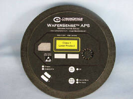
Moving through semiconductor process equipment, Airborne Particle Sensor monitors airborne particles, reporting back information in real-time to allow engineers to validate and analyze wafer contamination. Vacuum-compatible unit can detect 0.1 µm particles in multiple Bin schemes and does not require engineers to open chambers or expose ultra-clean process areas. Using companion software, particle data can be recorded to compare past to present operations as well as one tool to another.
Original Press Release:
CyberOptics Semiconductor To Demonstrate its New Airborne Particle Sensor
CyberOptics Semiconductor (www.cyberopticssemi.com) will demonstrate its new Airborne Particle Sensor (APS) for wafer processing equipment during Semicon Korea in booth number 1514. Semiconductor Software and Engineering Solutions (SESO), CyberOptics' distributor for Korea, will host the product demonstration as well as display CyberOptics WaferSense line of wireless metrology devices at the international trade show scheduled for January 26 - 28 in Seoul, Korea.
The Airborne Particle Sensor is a one-of-a kind, wafer-like technology that moves through semiconductor process equipment and automation material handing systems to monitor airborne particles, reporting back information in real-time to allow engineers to efficiently validate and analyze wafer contamination. By reducing the time and expense associated with process equipment particle qualification, the APS improves die yield and compresses final wafer inspection.
Fabs unable to isolate and mitigate the source of particles in a tool before wafer processing can use this sensor to efficiently detect and classify particles with their exact sources as wafers are transferred, slit valves actuate and chambers are cycled, pumped down and purged. With real-time views of particle conditions, process engineers can address specific trouble spots and be better prepared to pass particle qualifications on the very first attempt.
How it Works
The Airborne Particle Sensor uses a fan to pull non-corrosive gas or air through a channel as a laser illuminates the gas stream while particles scatter light onto the sensors photodiode. Compatible with front-ends, coater/developer tracks, deposition and etch equipment, the APS has the ability to detect 0.1 um particles in multiple Bin schemes. The automation-friendly, vacuum-compatible sensor doesn't require engineers to open chambers or expose ultra-clean process areas to the environment. The sensor can detect particles in real-time without opening the tool.
Using the sensor's companion software, ParticleView(TM) and ParticleReview(TM), fab engineers can collect and display particle data wirelessly to see the effect of adjustments in real time, speeding equipment qualification and setup. Particle data can be recorded to compare past to present operations as well as one tool to another to conduct machine-to-machine trend analysis of particle conditions and to establish process control and conduct process improvement.
Mr. Mark Hannaford, Director of Sales & Marketing of CyberOptics Semiconductor, will be in attendance at Semicon Korea along with Yukinobu Hayashi, Field Applications Engineer, to discuss the APS in booth number 1514. For more information on the Airborne Particle Sensor, please refer to our web site at www.cyberopticssemi.com/products/ or contact sales at (503) 495-2200 for more information.
About CyberOptics Semiconductor, Inc.
CyberOptics Semiconductor develops automated products that seamlessly measure critical parameters in semiconductor fabrication processes and equipment. The company's pioneering WaferSense® line includes wireless metrology devices for vibration, leveling, gapping, teaching and sensing airborne particles in semiconductor process equipment. The company is the largest producer of reflective wafermapping sensors and a leading provider of frame grabber machine vision boards under its HAMA Sensors(TM) and Imagenation(TM) brands. CyberOptics Semiconductor is a subsidiary of CyberOptics Corp. (Nasdaq:CYBE), one of the world's leading providers of process yield and throughput improvement solutions for the electronic assembly and semiconductor fabrication industries. For information, visit www.cyberopticssemi.com/, e-mail CSsales@cyberoptics.com or call 800-366-9131.