71131 XMC Module features 16-bit A/Ds.
Press Release Summary:
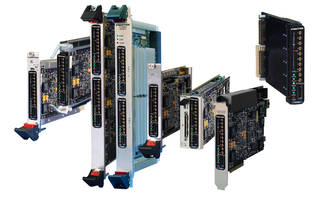
Featuring Xilinx Kintex UltraScale FPGA architecture, 71131 XMC Module is provided with eight A/D Acquisition IP Modules for capturing and moving data. Designed to operate with carrier boards in PCIe, 3U & 6U VPX, AMC, and 3U & 6U, XMC module comes with eight HF or IF input ports coupled to ADS42LB69 dual 250 MHz, 16-bit A/D converters. Unit comes with Navigator™ Design Suite and pre configured Pentek 8266 SPARK® PC, 8264 SPARK 6U VPX, or 8267 SPARK 3U VPX.
Original Press Release:
Pentek Announces 8-Channel A/D Jade XMC Module for Defense and Radar Phased-Array Applications
- Eight-channel, 250 MHz, 16-bit A/D XMC module with programmable multiband Digital Down Converters
- Jade Architecture with Xilinx Kintex Ultrascale FPGA offers price, power and processing performance advantages
- Navigator Design Suite compatible with Xilinx’s Plug-and-Play Vivado IP Integrator expedites development
Embedded Tech Trends Forum─Pentek, Inc., today introduced the newest member of the Jade™ family of high-performance data converter XMC modules based on the Xilinx Kintex Ultrascale FPGA. The Model 71131 is an eight-channel, 250 MHz XMC module featuring 16-bit A/Ds with programmable multiband digital down converters (DDCs).
The Model 71131 is suitable for connection to HF or IF ports of a communications or radar system. Its built-in data capture feature offers an ideal turnkey solution as well as a platform for developing and deploying custom FPGA-processing IP. The eight channels make it especially beneficial for multi-channel phased array platforms in defense and weather radar applications where the cost per channel can be substantially reduced.
A/D Converter Stage
The front end accepts eight analog HF or IF inputs on front panel MMCX connectors with transformer coupling into four Texas Instruments ADS42LB69 dual 250 MHz, 16-bit A/D converters. The digital outputs are delivered into the Kintex UltraScale FPGA for signal-processing and routing to other module resources.
Performance IP Cores
The Model 71131 features eight A/D Acquisition IP Modules for easily capturing and moving data. Each IP module can receive data from any of the eight A/Ds or a test signal generator. Powerful linked-list DMA engines move the A/D data through the PCIe interface in a unique Acquisition Gate Driven mode. In this mode, the length of a transfer performed by a link definition need not be known prior to data acquisition; rather, it is governed by the length of the acquisition gate. This is extremely useful in applications where an external gate drives acquisition and the exact length of that gate is not known or is likely to vary.
Within each A/D Acquisition IP Module is a powerful DDC IP core. Because of the flexible input routing of the A/D Acquisition IP Modules, many different configurations can be achieved including one A/D driving all eight DDCs or each of the eight A/Ds driving its own DDC.
Each DDC has an independent 32-bit tuning frequency setting that ranges from DC to the A/D sampling frequency. Each DDC can have its own unique decimation setting, supporting as many as eight different output bandwidths. Decimations can be programmed from 2 to 32,768, delivering bandwidths ranging from 100 MHz down to a few kHz to best suit each application.
“Our customers are excited to take advantage of the Jade Architecture and our Navigator Design Suite,” said Bob Sgandurra, director of Product Development of Pentek. “Access to over 90 Pentek IP modules using the AXI interface has greatly eased their design effort, reducing cost and development time while eliminating worries about complex data converter interface issues.”
The Jade Architecture
The Pentek Jade Architecture is based on the Xilinx Kintex UltraScale FPGA, which raises the digital signal processing (DSP) performance by over 50% with equally impressive reductions in cost, power dissipation and weight. As the central feature of the Jade Architecture, the FPGA has access to all data and control paths, enabling factory-installed functions including data multiplexing, channel selection, data packing, gating, triggering and memory control. A 5 GB bank of DDR4 SDRAM is available to the FPGA for custom applications. The Gen.3 x8 PCIe link can sustain 6.4 GB/s data transfers to system memory. Eight additional gigabit serial lanes and LVDS general purpose I/O lines are available for custom solutions.
Navigator Design Suite for Streamlined IP Development
Pentek’s Navigator™ Design Suite was designed from the ground up to work with Pentek’s Jade architecture and Xilinx’s Vivado Design Suite® providing an unparalleled plug-and-play solution to the complex task of IP and control software creation and compatibility. The Navigator Design Suite consists of two components: Navigator FDK (FPGA Design Kit) for integrating custom IP into Pentek sourced designs and Navigator BSP (Board Support Package) for creating host applications. Users can work efficiently at the API level for software development and with an intuitive graphical interface for IP design. The Navigator BSP is available for Windows and Linux operating systems.
Pre-Configured SPARK System Ready for Immediate Use
With a Pentek 8266 SPARK® PC, 8264 SPARK 6U VPX, or 8267 SPARK 3U VPX development system, work can begin immediately on applications. A SPARK system saves engineers time and expense associated with building and testing a development system and ensures optimum performance of Pentek boards. SPARK development systems are ready for immediate operation with software and hardware installed. In many applications, the SPARK development system can become the final deployed application platform.
Form Factors
The Model 71131 XMC module is designed to operate with a wide range of carrier boards in PCIe, 3U & 6U VPX, AMC, and 3U & 6U CompactPCI form factors, with versions for both commercial and rugged environments.
Pricing and Availability
Designed for air-cooled, conduction-cooled, and rugged operating environments, the Model 71131 XMC module with 5 GB of DDR4 SDRAM starts at $13,495 USD. Additional FPGA options are available. Delivery is 8 to 10 weeks ARO.
The Navigator Design Suite consists of two packages. The Navigator BSP is $2,500 USD and the Navigator FDK is $3,500 USD.
About Pentek
Pentek, an ISO 9001:2008 certified company, designs, manufactures and markets innovative COTS and rugged DSP boards and real-time recorders for commercial, government and military systems, including radar, communications, medical and industrial control applications. Pentek offers powerful VME, VPX, VXS, FMC, XMC, cPCI, PCIe and AMC boards for data acquisition, software radio and digital signal processing featuring Xilinx FPGAs. Pentek’s high-speed real-time recording systems are pre-configured and can be used in the lab or deployed in the field. Pentek equips all boards and recorder products with high-performance I/O including gigabit serial interfaces, powerful software development tools and offers strong DSP software support.
North American Sales Contact:
Mario Schiavone,
Pentek, Inc.,
One Park Way, Upper Saddle River, NJ 07458-2311;
201-818-5900;
Fax 201-818-5904;
Email news@pentek.com;
Website www.pentek.com.
International Sales Contacts:
Galleon Embedded Computing in Germany at (49) 89 5908 2101, LVD Systems in Italy at (39) 011 966 1319, Advanced Embedded Systems in the UK, Spain, France and Portugal at (44) 0 1202 885 675, Sela Electronic Systems in Israel at (972) 3 6479969, MISH International in Japan at (81) 42-538-7650, Nanjing Inspire Electronics Technology in China and Hong Kong at (86) 151 6147 0785, Acetronix Co. Ltd. in Korea at (82) 24202343, ext. 106, Dynamic C4 Pte. Ltd. in Singapore, Malaysia, Indonesia, Taiwan, Thailand and Vietnam at (65) 6405 4506, Unitronix Pty Ltd in Australia at (61) 2 4977 3511. For a list of Pentek representatives and distributors, please visit http://www.pentek.com/contact/replist.pdf