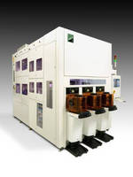
3D Electroplating System simplifies wafer level packaging.
Share:
Press Release Summary:
SABRE 3D electroplating system has modular architecture that delivers processes such as copper through-silicon vias, copper redistribution layers, pillars, under-bump metallization, and lead-free micro-bumping. Enabling multi-layer processing, system includes TurboCell(TM) technology for through-resist plating applications that improves film uniformity and alloy consistency. It also features in-line isotropic wet etch process that allows independent control of plated copper fill and overburden.
Original Press Release:
Novellus Introduces SABRE® 3D Electroplating System for the Advanced Wafer-Level Packaging Market
Highly Productive, Modular Platform Delivers Technology to Enable 3D Integration
SAN JOSE, Calif. - Novellus Systems (NASDAQ:NVLS) today introduced the SABRE 3D electroplating system for the rapidly-growing advanced wafer-level packaging (WLP) market. Utilizing technology from Novellus' industry-leading SABRE Electrofill® copper damascene interconnect system, SABRE 3D's flexible and modular architecture delivers a range of high-productivity WLP processes, including copper through-silicon vias (TSV), copper redistribution layers (RDL), pillars, under-bump metallization, and lead-free micro-bumping. The new SABRE 3D platform incorporates technological advances specifically designed to enable the tighter interconnect pitches, higher production yields, improved uniformities, and reduced costs driven by advanced WLP applications. TurboCell(TM) technology for high rate electroplating, Advanced Pretreatment Technology (APT(TM)) for robust wetting, and XMM(TM) overburden reduction are just some of the new innovations employed by SABRE 3D.
Strong demand for more powerful mobile electronics is driving the development of alternate packaging technologies that enable faster device speeds, increased functionality and I/O density, lower power consumption, and minimized form factor. 3D integration has emerged to meet these demands with the promise to be more cost-effective than conventional 2D scaling and is driving an ever-increasing need for innovation in WLP applications.
SABRE 3D was designed to meet the emerging needs of the advanced WLP market with an innovative, flexible, and modular architecture that maximizes footprint density, enables configurable multi-layer processing, and supports field extendibility for seamless capacity expansion. The field-configurable design also simplifies the transition from the development environment to high volume manufacturing. SABRE 3D incorporates many of the same technologies that have made the SABRE platform the industry-leader in electrochemical deposition reliability and manufacturability. SABRE's sealed dry contacts, innovative clamshell and cell design, SmartDose® bath control, and precision wafer handling have been integrated into the new SABRE 3D platform.
New technology innovations are central to SABRE 3D's benchmark-setting technical performance and productivity. Through targeted development of Electrofill chemistry and processes, SABRE 3D delivers void-free TSV fill and improves TSV integration by reducing thermally-induced via protrusion. Advanced Pretreatment Technology (APT) ensures robust wetting and consistent fill initiation, resulting in plating times up to 50 percent faster than competing offerings. Novellus' XMM technology, an in-line isotropic wet etch process, enables independent control of plated copper fill and overburden and reduces CMP cost of consumables by up to 70 percent. Additionally, Novellus has developed new, proprietary TurboCell technology for through-resist plating applications that dramatically improves film uniformity and alloy consistency while providing exceptionally high plating rates.
"The new SABRE 3D platform leverages over 12 years of industry-leading electroplating technology and experience to address the emerging requirements of the advanced WLP market," said Sesha Varadarajan, vice president and general manager of Novellus' Electrofill business unit. "SABRE 3D's innovative design and feature set support a range of applications for 3D integration where technology and cost are equally important."
About Novellus' ECD Technology:
For high-volume manufacturing applications at 45nm and beyond, Novellus' advanced copper electrochemical deposition hardware, processes, and chemistries combine industry-leading throughput with bottom-up void-free filling of advanced device structures. Nine out of ten copper interconnect wafers in the world are manufactured on Novellus SABRE Electrofill® systems.
About Novellus:
Novellus Systems, Inc. (NASDAQ:NVLS) is a leading provider of advanced process equipment for the global semiconductor industry. An S&P 500 company, Novellus is headquartered in San Jose, Calif. with subsidiary offices across the globe. For more information, please visit novellustechnews.com
Novellus, SABRE, Electrofill, and SmartDose are registered trademarks; and TurboCell, APT, and XMM are trademarks of Novellus Systems, Inc.
Source: Novellus Systems, Inc.
CONTACT: Bob Climo of Novellus Systems, Inc., +1-408-943-9700, bob.climo@novellus.com
Web Site: http://www.novellus.com/