ZEISS Highlights Scanning Electron Microscopes at EIPBN 2015
Share:
Visit Booth 113 to learn about ZEISS GeminiSEM and ZEISS MultiSEM 505 technology
ZEISS announces they will be highlighting a range of scanning electron microscope (SEM) technology at EIPBN, the 59th International Conference on Electron, Ion, and Photon Beam Technology and Nanofabrication, May 26-29, 2015, at the Manchester Grand Hyatt in San Diego, CA, Booth # 113. Stop by and learn more about ZEISS GeminiSEM field emission scanning electron microscope (FE-SEM) and ZEISS MultiSEM 505, the world’s fastest scanning electron microscope.
The ZEISS GeminiSEM family of microscopes are ideal for high contrast, low voltage images. The ZEISS GeminiSEM family provides flexible and reliable field emission SEM for research, industrial lab, or imaging facilities. Offering effortless imaging, ZEISS GeminiSEM allows users to achieve sub-nanometer resolution and high detection efficiency, even in variable pressure mode. ZEISS GeminiSEM 500 combines proven Gemini technology with a novel electron optical design. Users can achieve better resolution, especially at low voltage. With 20 times greater in-lens detection signal, crisp images can be obtained fast and with minimum sample damage. With the new variable pressure mode, users feel as if they are working in high vacuum.
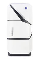
ZEISS MultiSEM 505, the world’s fastest scanning electron microscope, unleashes the acquisition speed of 61 parallel electron beams. Samples can be imaged in the centimeter scale at nanometer resolution. This unique SEM is designed for continuous, reliable 24/7 operation. Simply set up a high-throughput data acquisition workflow and ZEISS MultiSEM 505 will acquire high contrast images automatically. Control ZEISS MultiSEM 505 with proven ZEN imaging software, featuring smart auto-tuning routines support and the ability to quickly and easily set up complex automated acquisition procedures, adapted and tuned to specific samples.
About ZEISS
ZEISS is an internationally leading technology enterprise operating in the optics and optoelectronics industries. ZEISS develops and distributes lithography optics, measuring technology, microscopes, medical technology, eyeglass lenses, camera and cine lenses, binoculars and planetarium technology. With its solutions, the company constantly advances the world of optics and helps shape technological progress. The company is divided up into the six business groups Industrial Metrology, Microscopy, Medical Technology, Vision Care, Consumer Optics and Semiconductor Manufacturing Technology. ZEISS is represented in over 40 countries – with around 30 production sites, over 50 sales and service locations and about 25 research and development facilities. In fiscal year 2013/14 the company generated revenue approximating 4.3 billion euros with just under 25,000 employees. Founded in 1846 in Jena, the company is headquartered in Oberkochen, Germany. Carl Zeiss AG is the strategic management holding company that manages the ZEISS Group. The company is wholly owned by the Carl Zeiss Stiftung (Carl Zeiss Foundation).
Further information at www.zeiss.com
Microscopy
The Microscopy business group is the world's only one-stop manufacturer of light, X-ray and electron microscope systems. The portfolio includes solutions and services both for life sciences and materials research and for industry, education and clinical practice. The business group is headquartered in Jena. Additional production and development sites are located in Oberkochen, Göttingen and Munich in Germany, as well as in Cambridge in the UK, and in Peabody, MA and Pleasanton, CA in the USA. The business group employs a total of over 3,000 people. It generated revenue of 656 million euros in fiscal year 2013/14.
Press contact
Microscopy
Maya Everett, Ph.D.
Phone +1 914 681-7782
Email: maya.everett@zeiss.com
www.zeiss.com/press