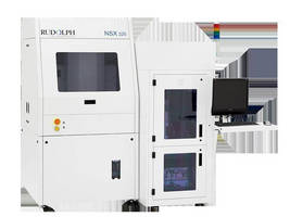
Rudolph Ships New NSX 320 TSV Metrology System to CEA-Leti for through Silicon Via Process Development
First NSX 320 Metrology system sold specifically for TSV application includes specialized sensors to measure critical parameters in 3D integration
Flanders, New Jersey — Rudolph Technologies, Inc. (NYSE: RTEC) announced today the sale of its first NSX® 320 TSV Metrology System to CEA-Leti, a leading research organization based in Grenoble, France, which, in the frame of the Nanoelec Research Technology Institute (Nanoelec RTI) program, is developing three-dimensional integrated circuit (3DIC) technologies that use through silicon vias (TSVs) to conduct signals among vertically-stacked chips. The new NSX 320 TSV system includes integrated 3D metrology that enables specialized measurements critical to the TSV process.
"Controlling the processes used to create TSVs requires a number of specialized measurements, such as the total thickness variation (TTV) of the wafer bonded to the carrier, or the remaining silicon thickness after thinning," said Séverine Cheramy, CEA-Leti's director of 3D integration development in the Nanoelec RTI program. "The NSX system's 3D metrology capabilities, which combine accurate 2D measurements with the ability to see and measure front, back and internal interface surfaces, will provide critical information for our TSV development program."
Matt Wilson, Rudolph's NSX Series product manager adds, "Three-dimensional integration using TSVs is widely expected to be a key technology enabling our industry to maintain the incredible pace of development and innovation first described as Moore's Law nearly 50 years ago. Ultimately we see the potential for rapid growth in this segment and are pleased to be part of the pioneering efforts of a leading research organization like CEA-Leti."
Rudolph's NSX TSV metrology systems combine the NSX family's well-established 2D inspection capabilities with an advanced 3D metrology that was developed at recently-acquired Tamar Technology. Together, they allow the NSX metrology system to perform a wide variety of measurements needed to characterize and control TSV processes, including TSV depth measurements, bottom CD measurements, pre- and post-thinning remaining silicon thickness measurements during the reveal process, copper nail height measurements, edge trim monitoring, adhesive TTV of bonded pairs and product wafers, and traditional defect inspection throughout the entire process.
For more information about Rudolph's NSX Metrology Series, please visit www.rudolphtech.com.
About CEA-Leti
By creating innovation and transferring it to industry, Leti is the bridge between basic research and production of micro- and nanotechnologies that improve the lives of people around the world. Backed by its portfolio of 2,200 patents, Leti partners with large industrials, SMEs and startups to tailor advanced solutions that strengthen their competitive positions. It has launched more than 50 startups. Its 8,000m² of new-generation cleanroom space feature 200mm and 300mm wafer processing of micro and nano solutions for applications ranging from space to smart devices. Leti's staff of more than 1,700 includes 200 assignees from partner companies. Leti is heading the Nanoelec RTI program which benefits from French State aid under the "Programme Investissements d'Avenir" agreement bearing reference ANR-10-AIRT-05. Leti is based in Grenoble, France, and has offices in Silicon Valley, Calif., and Tokyo. Visit www.leti.fr for more information.
About Rudolph Technologies
Rudolph Technologies, Inc. is a worldwide leader in the design, development, manufacture and support of defect inspection, advanced packaging lithography, process control metrology, and data analysis systems and software used by semiconductor device manufacturers worldwide. Rudolph provides a full-fab solution through its families of proprietary products that provide critical yield-enhancing information, enabling microelectronic device manufacturers to drive down the costs and time to market of their products. The Company's expanding portfolio of equipment and software solutions is used in both the wafer processing and final manufacturing of ICs, and in adjacent markets such as FPD, LED and Solar. Headquartered in Flanders, New Jersey, Rudolph supports its customers with a worldwide sales and service organization. Additional information can be found on the Company's website at www.rudolphtech.com.
Contacts:
Trade Press:
Amy Pauling
952.259.1794
amy.pauling@rudolphtech.com
CEA-Leti:
Pierre-Damien Berger
+33 4 38 78 02 26
Pierre-damien.berger@cea.fr