MIRTEC to Preview the MP-520 Advanced System in Package (SiP) Inspection and Measurement System at SEMICON West 2015
Share:
MIRTEC, "The Global Leader in Inspection Technology," will exhibit its most recent solutions for System in Package (SiP) inspection and measurement at SEMICON WEST 2015; July 14-16, 2015, at the Moscone Center in San Francisco, CA. Visitors are invited to booth # 2343 for a detailed demonstration of this exciting new technology.
Brian D’Amico president of MIRTEC’s North American Sales and Service Division stated; “The growing demand for miniaturization and higher functionality at reduced production costs has led to the industry requirement of System in Package (SiP) solutions. An SiP is a number of integrated circuits enclosed in a single package. The SiP performs all or most of the functions of an electronic system. These packages are typically used in mobile devices such as cell phones and digital music players. Dies containing integrated circuits may be stacked vertically on a substrate and are internally connected by wire bond to the package. Alternatively, with a flip chip technology, solder bumps are used to join stacked chips together. As one can imagine, this complex arrangement of advanced packaging presents a challenge to the inspection environment.”
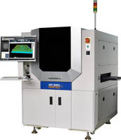
MIRTEC’s MP-520 system was developed specifically to address the challenges related to SiP inspection. The MP-520 combines Precision Linear Drive Motor Technology with MIRTEC’s exclusive 25 Mega Pixel CoaXPress Camera System, a 3D Confocal Measurement system and revolutionary OMNI-VISION 3D Digital Multi-Frequency Moiré Technology to provide high-speed, high-resolution inspection and measurement for SiP and other semiconductor applications. The MP-520 also is configured with eight (8) phase color lighting and four (4) 10 Mega Pixel side-view cameras.
The MP-520 is suitable for measurement and inspection of the following manufacturing criteria:
• Solder Ball/Bump – Presence, Pitch, Offset, Height, Co-Planarity and Bridging
• Bond Wire - Short, Broken, Shift and Loop Height
• Chip Bond - Offset, Height, Crack and Chip
• Discrete Device – Presence, Offset, Height, Co-Planarity and Solder Fillet
• Heat Sink - Presence, Offset and Height
• Under-Fill – Presence, Fillet and Height
• PCB - Scratch, Contamination and Bridging
• Package - Warpage, Crack, Marking, Dimensions and Chipping
Inspection and measurement results are stored in a central database, enabling customers to remotely access SPC data through MIRTEC’s INTELLISYS total quality management system software. This software suite promotes continuous process improvement by allowing the manufacturers to track and eliminate defects on inspected assemblies. INTELLISYS also provides remote debugging and monitoring of up to eight production lines, allowing MIRTEC customers to further maximize the efficiency of the inspection process.
“MIRTEC has gained a solid reputation in the semiconductor inspection industry by providing unprecedented performance, quality and cost-effectiveness to the manufacturing environment,” continued D’Amico, “We have achieved a high level of customer satisfaction with a growing number of global semiconductor companies for our advanced back-end inspection solutions. We look forward to welcoming visitors to our booth # 2343 during the three-day event.”
MIRTEC is a leading global supplier of automated optical inspection systems to the electronics manufacturing industry. For further information, please visit www.mirtecusa.com.
Contact:
Brian D’Amico
MIRTEC Corp
Phone: 203-881-5559
E-mail: bdamico@mindspring.com
Web: www.mirtecusa.com