KLA-Tencor Announces New Flagship Wafer Inspection Solution Suite to Support Advanced Design-Rule Chip Manufacturing: 2900 Series, Puma 9650 Series, eS800 Series
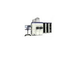
MILPITAS, Calif. - Today KLA-Tencor Corporation (NASDAQ: KLAC), announced three new wafer defect inspection systems for leading-edge chip manufacturers: the 2900, Puma 9650 and eS800 systems. This new flagship suite is designed to address the wide range of defect issues that new materials, structures and design rules have imposed on manufacturers of advanced chips. The new 2900 Series broadband optical wafer defect inspection platform extends optical wafer defect inspection to new limits, with significant strides forward in defect capture on challenging layers and die areas, and capture of yield-relevant defects as small as 10nm. Complementing the 2900 is the new Puma 9650Series narrowband optical wafer defect inspection system, which advances the Puma product line's unique combination of sensitivity and throughput to new heights of performance on many layers, including difficult gate etch layers. To capture extremely small defects or shallow residues, or defects inside deep, narrow structures, the new eS800 Series e-beam wafer defect inspection platform can leverage its proprietary design for achieving high electron beam current density.
Each of the inspection systems in the new portfolio features seamless connectivity to the recently introduced eDR-7000 e-beam wafer defect review system. With outstanding sensitivity and review speed, the eDR-7000 completes the process of identifying the defect types found by the inspectors, allowing engineers to address defect issues promptly and disposition wafers accurately.
"Our leading-edge customers have a wide variety of defect problems to solve, the most difficult of which involve finding tiny or subtle defects amidst pattern noise, deep inside a capacitor, or in otherwise difficult environments," said Mike Kirk, Ph.D., group vice president of the Wafer Inspection Group at KLA-Tencor. "The trio of new inspection systems that we are announcing today incorporates exceptional work by our engineering teams: new, more powerful light sources or electron guns, innovative signal shaping and a multifold approach to reducing noise. The resulting advancements in signal-to-noise are impressive for each tool. We believe that these three products will play a vital role in enabling our customers to bring their next-generation logic and memory devices to market."
The 2900Series broadband optical wafer defect inspection platform delivers increased capture of small defects of interest on early process layers and back-end layers, with sensitivity approaching that of e-beam inspection in some cases. Its overall defect capture on after-develop inspection (ADI) layers rivals that of after-etch inspection (AEI) results. The tool's dramatically improved ADI performance means that the fab can identify killer defects earlier in the process, allowing engineers to correct the issue before more time and material have been wasted. These performance breakthroughs are enabled by innovations throughout the system, including:
o Second-generation PowerBroadband(TM), a laser-pumped plasma light source that delivers about twice the light of the 2830's original PowerBroadband source;
o New optics providing significant resolution improvement at DUV wavelengths and dramatic optical noise reduction;
o New two-dimensional Directional E-Field(TM), new brightfield and darkfield apertures, and new wavelength bands that can boost defect signal and/or reduce wafer noise;
o New, seamlessly integrated XP design-aware recipe setup and defect detection, for improved yield relevance of inspection results;
o New image computer, supporting increased throughput and algorithm advancements;
o Redesigned stage, helping provide a significant improvement in defect location accuracy, for better and more efficient defect review; and
o New 12-bit dynamic range, enabling increased defect capture in high-contrast areas such as memory transition regions.
Further details about the 2900 can be found on the product web page at: www.kla-tencor.com/front-end-defect-inspection/29xx-series.html.
The Puma 9650 Series narrowband optical wafer defect inspection systems provide improved defect capture in yield-critical die areas, such as the edges of SRAM arrays, memory transition regions and page breaks. Upgradeable from the industry-leading Puma 9550 platform, the new Puma provides overall higher sensitivity to particles and pattern defects including bridges, residue and extra pattern on front-end etch layers. These performance enhancements to the Puma platform are enabled by the following engineering advances:
o Smaller pixel to boost sensitivity to small defects, such as trench residue and extra pattern defects;
o Innovations in pupil engineering to enhance sensitivity around cell edges;
o New eFence(TM) technology to suppress interference from repeating patterns in page break and transition regions;
o Improvements to pattern suppression technology throughout the die; and
o Extended dynamic range, to improve system response near array edges and in the periphery.
Further details about the Puma 9650 can be found on the product web page at: www.kla-tencor.com/front-end-defect-inspection/puma-family.html.
The eS800Series e-beam inspection systems feature leading-edge physical and electrical defect capture on a wide range of layers and structures, the most challenging of which include defects inside deep trenches and vias, or at the very edges of DRAM and SRAM arrays. Moreover, the eS800 offers the throughput needed to scan large areas of the die to find electrical defect signatures such as under-etch, shorts or opens. In order to meet the performance targets for this tool, KLA-Tencor's e-beam technology group developed and implemented several technology enhancements over the previous-generation eS3X tools, including:
o New electron gun and breakthrough, proprietary optics that allow a higher beam current density in a smaller spot size, enabling higher sensitivity overall, the ability to inspect defects inside high aspect-ratio structures and higher throughput;
o Wider operating conditions that allow better performance on less conductive layers such as low-k dielectrics, and better capture of subtle residue and under-etch defects;
o TurboScan(TM)( )methodology for inspecting contacts in NAND flash at up to ten times the speed of the eS35; and
o Ability to capture both physical and electrical (voltage-contrast) defects with critical sensitivity in a single e-beam inspection system, allowing fabs flexibility in work routing and cost-effective use of this high-end inspection system.
Further details about the eS800 can be found on the product web page at: www.kla-tencor.com/front-end-defect-inspection/es800-series.html.
The 2900, Puma 9650 and eS800 tools share an intuitive graphical user interface, for ease of operator training, flexible work routing and faster time to production integration. All three tools can be seamlessly linked to KLA-Tencor's eDR-7000 e-beam wafer defect review system-an indispensable partner for fast, accurate defect review and classification. To maintain high performance and productivity, the 2900, Puma 9650 and eS800 Series systems are backed by KLA-Tencor's global, comprehensive service network.
The 2900, Puma 9650 and eS800 tools have been shipped to leading foundry, logic and memory chip manufacturers for use in advanced development and production lines.
About KLA-TencorKLA-Tencor Corporation, a leading provider of process control and yield management solutions, partners with customers around the world to develop state-of-the-art inspection and metrology technologies. These technologies serve the semiconductor, data storage, LED, photovoltaic, and other related nanoelectronics industries. With a portfolio of industry-standard products and a team of world-class engineers and scientists, the company has created superior solutions for its customers for more than 35 years. Headquartered in Milpitas, Calif., KLA-Tencor has dedicated customer operations and service centers around the world. Additional information may be found at www.kla-tencor.com. (KLAC-P)
SOURCE KLA-Tencor Corporation
CONTACT: Meggan Powers, Sr. Director, Corporate Communications, +1-408-875-8733, meggan.powers@kla-tencor.com
Web Site: www.kla-tencor.com